2SK3147(L), 2SK3147(S)
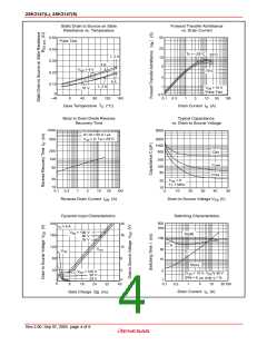
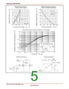
Reverse Drain Current vs.
Source to Drain Voltage
Maximum Avalanche Energy vs.
Channel Temperature Derating
10
8
2.5
2.0
1.5
1.0
IAP= 5 A
VDD = 50 V
duty < 0.1 %
Rg > 50 Ω
6
10 V
4
VGS = 0, –5 V
5 V
2
0.5
0
Pulse Test
1.6 2.0
0
0.4
0.8
1.2
25
50
75
100
125
150
Source to Drain Voltage VSD (V)
Channel Temperature Tch (°C)
Normalized Transient Thermal Impedance vs. Pulse Width
3
1
Tc = 25°C
D = 1
0.5
0.3
0.1
θ
θ
γ
θ
ch – c(t) = s (t) • ch – c
ch – c = 6.25°C/W, Tc = 25°C
PW
T
P
DM
D =
0.03
0.01
PW
T
10 µ
100 µ
1 m
10 m
100 m
1
10
Pulse Width PW (S)
Avalanche Test Circuit
Avalanche Waveform
VDSS
L
1
2
2
EAR
=
• L • IAP •
VDS
Monitor
VDSS – VDD
IAP
Monitor
V(BR)DSS
IAP
Rg
VDS
VDD
D. U. T
I
D
Vin
15 V
50 Ω
VDD
0
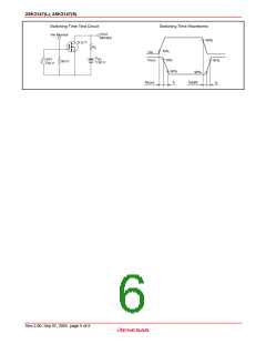
Rev.2.00 Sep 07, 2005 page 5 of 8

 RENESAS [ RENESAS TECHNOLOGY CORP ]