2SK3147(L), 2SK3147(S)
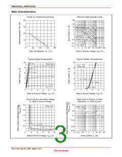
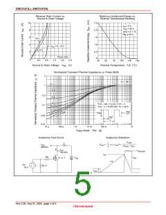
Static Drain to Source on State
Resistance vs. Temperature
Forward Transfer Admittance
vs. Drain Current
50
0.50
0.40
0.30
0.20
0.10
Pulse Test
20
10
5
Tc = –25°C
25°C
1, 2 A
5 A
VGS = 4 V
75°C
2
5 A
1, 2 A
1
VDS = 10 V
Pulse Test
10 V
0
0.5
–40
0
40
80
120
160
0.1 0.3
1
3
10
30
100
Case Temperature TC (°C)
Drain Current ID (A)
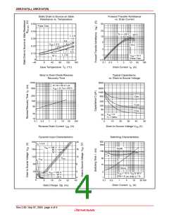
Body to Drain Diode Reverse
Recovery Time
Typical Capacitance
vs. Drain to Source Voltage
1000
500
5000
di / dt = 50 A / µs
VGS = 0, Ta = 25°C
2000
1000
500
200
100
50
Ciss
200
Coss
Crss
100
50
20
10
VGS = 0
20
10
f = 1 MHz
0.1 0.3
1
3
10
30
100
0
10
20
30
40
50
Reverse Drain Current IDR (A)
Drain to Source Voltage VDS (V)
Dynamic Input Characteristics
ID = 5 A
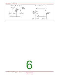
Switching Characteristics
500
300
200
160
120
80
20
VDD = 100 V
50 V
25 V
t
d(off)
16
12
8
100
t
f
VGS
30
10
VDS
t
r
t
d(on)
40
4
0
3
1
VDD = 100 V
50 V
25 V
VGS = 10 V, VDD = 30 V
PW = 5 µs, duty < 1 %
0
3
1
8
16
24
32
40
0.1
0.3
10
30100
Drain Current ID (A)
Gate Charge Qg (nc)
Rev.2.00 Sep 07, 2005 page 4 of 8

 RENESAS [ RENESAS TECHNOLOGY CORP ]