RTL8201CL
Datasheet
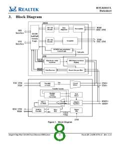
5. Pin Descriptions
LI: Latched Input during Power up or Reset
O: Output
P: Power
I: Input
IO: Bi-directional input and output
5.1. MII Interface
Table 1. MII Interface
Description
Transmit Clock.
Name
Type
Pin No.
TXC
O
7
This pin provides a continuous clock as a timing reference for TXD[3:0] and
TXEN.
TXEN
TXD[3:0]
RXC
I
I
2
Transmit Enable.
The input signal indicates the presence of valid nibble data on TXD[3:0]. An
internal weak pull low resistor prevents the bus floating.
Transmit Data.
The MAC will source TXD[0..3] synchronous with TXC when TXEN is
asserted. An internal weak pull high resistor prevents the bus floating.
Receive Clock.
This pin provides a continuous clock reference for RXDV and RXD[0..3]
signals. RXC is 25MHz in 100Mbps mode and 2.5Mhz in 10Mbps mode.
Collision Detect.
3, 4, 5, 6
O
16
1
COL
LI/O
COL is asserted high when a collision is detected on the media.
During power on reset, this pin status is latched to determine at which LED
mode to operate:
0: CL LED mode
1: BL LED mode
An internal weak pull low resistor sets this to the default CL LED mode. It is possible
to use an external 5.1KΩ pull high resistor to enable BL LED mode.
Carrier Sense.
This pin’s signal is asserted high if the media is not in Idle state.
An internal weak pull low resistor sets this to normal operation mode. An external
5.1KΩ pull low resistor could be reserved to ensure operating at normal mode.
Receive Data Valid.
CRS
LI/O
O
23
22
RXDV
This pin’s signal is asserted high when received data is present on the
RXD[3:0] lines. The signal is de-asserted at the end of the packet. The signal is
valid on the rising edge of the RXC.
RXD[3:0]
O
18, 19, 20, 21 Receive Data.
These are the four parallel receive data lines aligned on the nibble boundaries
driven synchronously to the RXC for reception by the external physical unit
(PHY).
Single-Chip/Port 10/100 Fast Ethernet PHYceiver
4
Track ID: JATR-1076-21 Rev. 1.24

 REALTEK [ Realtek Semiconductor Corp. ]