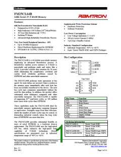
FM25CL64B - 64Kb 3V SPI F-RAM
high performance serial communication to a host
microcontroller. Many common microcontrollers
have hardware SPI ports allowing a direct interface.
It is quite simple to emulate the port using ordinary
port pins for microcontrollers that do not. The
FM25CL64B operates in SPI Mode 0 and 3.
Overview
The FM25CL64B is a serial F-RAM memory. The
memory array is logically organized as 8,192 x 8 and
is accessed using an industry standard Serial
Peripheral Interface or SPI bus. Functional operation
of the F-RAM is similar to serial EEPROMs. The
major difference between the FM25CL64B and a
serial EEPROM with the same pinout is the F-
RAM’s superior write performance.
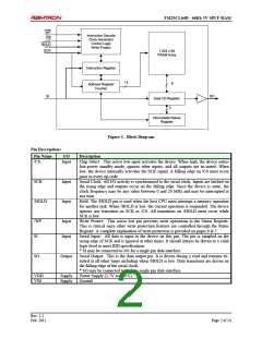
The SPI interface uses a total of four pins: clock,
data-in, data-out, and chip select. A typical system
configuration uses one or more FM25CL64B devices
with a microcontroller that has a dedicated SPI port,
as Figure 2 illustrates. Note that the clock, data-in,
and data-out pins are common among all devices.
The Chip Select and Hold pins must be driven
separately for each FM25CL64B device.
Memory Architecture
When accessing the FM25CL64B, the user addresses
8,192 locations of 8 data bits each. These data bits
are shifted serially. The addresses are accessed using
the SPI protocol, which includes a chip select (to
permit multiple devices on the bus), an op-code, and
a two-byte address. The upper 3 bits of the address
range are ‘don’t care’ values. The complete address
of 13-bits specifies each byte address uniquely.
For a microcontroller that has no dedicated SPI bus, a
general purpose port may be used. To reduce
hardware resources on the controller, it is possible to
connect the two data pins (SI, SO) together and tie
off (high) the /HOLD pin. Figure 3 shows a
configuration that uses only three pins.
Most functions of the FM25CL64B either are
controlled by the SPI interface or are handled
automatically by on-board circuitry. The access time
for memory operation is essentially zero, beyond the
time needed for the serial protocol. That is, the
memory is read or written at the speed of the SPI bus.
Unlike an EEPROM, it is not necessary to poll the
device for a ready condition since writes occur at bus
speed. So, by the time a new bus transaction can be
shifted into the device, a write operation will be
complete. This is explained in more detail in the
interface section.
Protocol Overview
The SPI interface is a synchronous serial interface
using clock and data pins. It is intended to support
multiple devices on the bus. Each device is activated
using a chip select. Once chip select is activated by
the bus master, the FM25CL64B will begin
monitoring the clock and data lines. The relationship
between the falling edge of /CS, the clock and data is
dictated by the SPI mode. The device will make a
determination of the SPI mode on the falling edge of
each chip select. While there are four such modes, the
FM25CL64B supports Modes 0 and 3. Figure 4
shows the required signal relationships for Modes 0
and 3. For both modes, data is clocked into the
FM25CL64B on the rising edge of SCK and data is
expected on the first rising edge after /CS goes
active. If the clock begins from a high state, it will
fall prior to beginning data transfer in order to create
the first rising edge.
Users expect several obvious system benefits from
the FM25CL64B due to its fast write cycle and high
endurance as compared with EEPROM. In addition
there are less obvious benefits as well. For example
in a high noise environment, the fast-write operation
is less susceptible to corruption than an EEPROM
since it is completed quickly. By contrast, an
EEPROM requiring milliseconds to write is
vulnerable to noise during much of the cycle.
The SPI protocol is controlled by op-codes. These
op-codes specify the commands to the device. After
/CS is activated the first byte transferred from the bus
master is the op-code. Following the op-code, any
addresses and data are then transferred. Note that the
WREN and WRDI op-codes are commands with no
subsequent data transfer.
Note: The FM25CL64B contains no power
management circuits other than a simple internal
power-on reset circuit. It is the user’s
responsibility to ensure that VDD is within
datasheet tolerances to prevent incorrect
operation. It is recommended that the part is not
powered down with chip enable active.
Important: The /CS pin must go inactive after an
operation is complete and before a new op-code
can be issued. There is one valid op-code only per
active chip select.
Serial Peripheral Interface – SPI Bus
The FM25CL64B employs
a Serial Peripheral
Interface (SPI) bus. It is specified to operate at speeds
up to 20 MHz. This high-speed serial bus provides
Rev. 1.2
Feb. 2011
Page 3 of 14

 RAMTRON [ RAMTRON INTERNATIONAL CORPORATION ]