lowers susceptibility to EMI, and yet permits excellent
response time. Internally the signals are digitally processed to
reject impulse noise, using a 'consensus' filter which requires
several consecutive confirmations of a detection before the
output is activated.
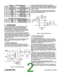
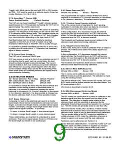
Table 1-1 Pin Descriptions
Pin
1
Name
/CAL_CLR
/SYNC_O
SNS1
Function
Ext Cal, latch clear input
Sync Output
2
3
Sense 1 line
A unique cloning process allows the internal eeprom of the
device to be programmed to permit unique combinations of
sensing and processing functions.
4
VSS
Negative supply (ground)
Sense 2 line
Sync Input
5
SNS2
/SYNC_I
OUT
6
7
Detection output
Positive supply
+2 to 5 Vdc
100nF
8
8
VDD
VDD
Alternate Pin Functions for Cloning
10K 10K
3
6
7
SCK
SDO
SDI
Serial clone data clock
Serial clone data out
Serial clone data in
Calibration
1
6
7
2
3
5
/CAL
SYNC_O
SNS1
SYNC_I
OUT
ELECTRODE
Cs
Cx
SNS2
4.7nF
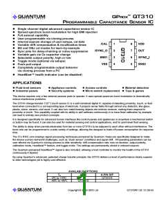
1 - OVERVIEW
The QT310 is a digital burst mode charge-transfer (QT)
sensor designed for touch controls, level sensing and
proximity sensing; it includes all hardware and signal
processing functions necessary to provide stable sensing
under a wide variety of changing conditions. Only one low
cost sampling capacitor is required for operation.
VSS
4
A unique aspect of the QT310 is the ability of the designer to
‘clone’ a wide range of user-defined setups into the part’s
eeprom during development and in production. Cloned setups
can dramatically alter the behavior of the part. For production,
the parts can be cloned in-circuit or can be procured from
Quantum pre-cloned.
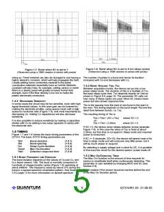
Figure 1-1 Basic QT310 circuit
1.2 ELECTRODE DRIVE
1.2.1 SWITCHING
O
PERATION
Figure 1-1 shows the basic QT310 circuit using the device,
with a conventional output drive and power supply
connections.
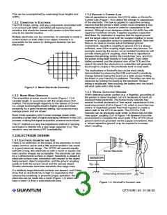
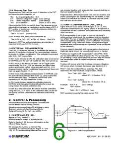
The IC implements direct-to-digital capacitance acquisition
using the charge-transfer method, in a process that is better
understood as a capacitance-to-digital converter (CDC). The
QT switches and charge measurement functions are all
internal to the IC (Figure 1-2).
1.1 BASIC OPERATION
The QT310 employs bursts of charge-transfer cycles to
acquire its signal. Burst mode permits power consumption in
the microamp range, dramatically reduces RF emissions,
The CDC treats sampling capacitor Cs as a floating store of
accumulated charge which is switched between the sense
pins; as a result, the sense electrode can be connected to
either pin with no performance difference. In both cases the
rule Cs >> Cx must be observed for proper operation. The
polarity of the charge build-up across Cs during a burst is the
same in either case. Typical values of Cs range from 10nF to
200nF.
Result
SNS1
Larger values of Cx cause charge to be transferred into Cs
more rapidly, reducing available resolution and resulting in
lower gain. Conversely, larger values of Cs reduce the rise of
differential voltage across it, increasing available resolution
and raising gain. The value of Cs can thus be increased to
allow larger values of Cx to be tolerated (Figures 5-1 to 5-2).
Cs
Cx
Start
Done
As Cx increases, the length of the burst decreases resulting in
lower signal numbers.
SNS2
The electrode should always be connected to SNS1;
connections to SNS2 are also possible but this can cause the
signal to be susceptible to noise.
Charge
Amp
It is important to limit the amount of stray Cx capacitance on
both SNS terminals, especially if the Cx load is already large.
Figure 1-2 Internal Switching
LQ
2
QT310/R1.03 21.09.03

 QUANTUM [ QUANTUM RESEARCH GROUP ]