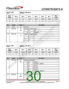
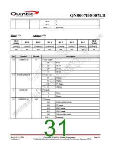
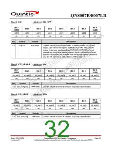
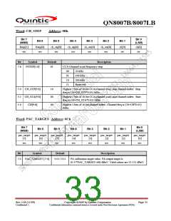
QN8007B/8007LB
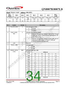
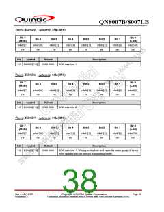
Word: TXAGC GAIN Address: 0Dh (RW)
Bit 7
(MSB)
Bit 0
(LSB)
Bit 6
Bit 5
Bit 4
Bit 3
Bit 2
Bit 1
tx_sftclpen
tagc_gain_
sel
rsvd
txagc
_gdb
txagc_gvga
[3]
txagc_gvga
[2]
txagc_gvga
[1]
txagc_gvga
[0]
wo
wo
rw
rw
rw
rw
rw
rw
Bit
Symbol
Default
Description
7
TX_SFTCLPEN
0
TX soft clipping enable:
0
1
Disable
Enabled
6
TAGC_GAIN_
SEL
0
TX AGC Gain selection method:
0
Both the TX digital gain TXAGC_GDB and the TX input
buffer gain TXAGC_GVGA [3:0] are determined by TX
AGC FSM on chip.
1
Both the TX digital gain and the TX input buffer gain are
determined by the contents of TXAGC_GDB and
TXAGC_GVGA [3:0] respectively.
5
4
rsvd
0
0
Reserved
TXAGC_GDB
TX digital gain:
0
1
0 dB
1 dB
3:0
TXAGC_GVGA
[3:0]
0001
TX input buffer gain: (dB)
VGAG
RIN[1:0]
[3:0]
00
01
-1.5
0
10
-7.5
-6
11
-13.5
-12
-10.5
-9
0000
0001
0010
0011
0100
0101
0110
0111
1000
1001
1010
1011
11XX
4.5
6
7.5
9
1.5
3
-4.5
-3
10.5
12
4.5
6
-1.5
0
-7.5
-6
13.5
15
7.5
9
1.5
3
-4.5
-3
16.5
18
10.5
12
13.5
15
4.5
6
-1.5
0
19.5
21
7.5
9
1.5
3
Reserved
Rev 2.09 (11/09)
Confidential A
Copyright ©2009 by Quintic Corporation
Confidential Information contained herein is covered under Non-Disclosure Agreement (NDA).
Page 34

 QUANTUM [ QUANTUM RESEARCH GROUP ]