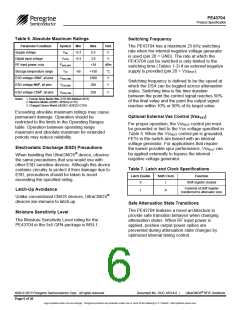
PE43704
Product Specification
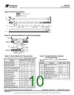
Figure 5. Serial Timing Diagram
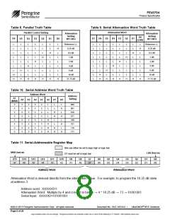
Bits can either be set to logic high or logic low
D[7] must be set to logic low
DI[6:0]
T
T
T
DISU
DIH
P/S
T
PSSU
PSIH
D[0]
D[1]
D[2]
D[3]
D[4]
D[5]
D[6]
D[7]
SI
T
SISU
T
SIH
CLK
T
T
T
LESU
CLKL
CLKH
LE
T
LEPW
T
PD
DO[6:0]
VALID
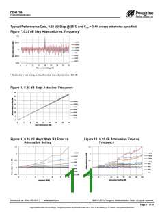
Figure 6. Latched-Parallel/Direct-Parallel Timing Diagram
P/S
TPSSU
TPSH
VALID
DI[6:0]
TDISU
TDIH
LE
TLEPW
VALID
TPD
DO[6:0]
TDIPD
Table 12. Serial Interface AC Characteristics
Table 13. Parallel and Direct Interface
AC Characteristics
VDD = 3.4V or 5.0V, -40°C < TA < 85°C, unless otherwise specified
VDD = 3.4V or 5.0V, -40°C < TA < 85°C, unless otherwise
specified
Parameter
Serial clock frequency
Serial clock HIGH time
Serial clock LOW time
Symbol
FCLK
Min
-
Max
Unit
MHz
ns
10
-
Symbol
Parameter
Min
Max
Unit
TCLKH
TCLKL
30
30
Latch enable minimum pulse
width
TLEPW
30
-
ns
-
ns
Last serial clock rising edge setup
time to Latch Enable rising edge
TDISU
TDIH
Parallel data setup time
Parallel data hold time
100
100
100
100
-
-
-
ns
ns
ns
ns
ns
TLESU
10
-
ns
Latch enable min. pulse width
Serial data setup time
Serial data hold time
TLEPW
TSISU
TSIH
30
10
-
-
ns
ns
ns
ns
ns
ns
ns
ns
ns
ns
TPSSU
TPSIH
TPD
Parallel/serial setup time
Parallel/serial hold time
Digital register delay (internal)
-
-
10
-
10
Parallel data setup time
Parallel data hold time
Address setup time
TDISU
TDIH
100
100
100
100
100
100
-
-
Digital register delay (internal,
direct mode only)
TDIPD
-
5
ns
-
TASU
TAH
-
Address hold time
-
Parallel/serial setup time
Parallel/serial hold time
Digital register delay (internal)
TPSSU
TPSH
TPD
-
-
10
©2012-2013 Peregrine Semiconductor Corp. All rights reserved.
Document No. DOC-16514-6 |
UltraCMOS® RFIC Solutions
Page 10 of 20
Logo updated under non-rev change. Peregrine products are protected under one or more of the following U.S. Patents: http://patents.psemi.com

 PSEMI [ Peregrine Semiconductor ]