TOP242-249
Conditions
(Unless Otherwise Specified)
See Figure 53
Parameter
Symbol
Min
Typ Max
Units
SOURCE = 0 V; TJ = -40 to 125 °C
SUPPLY VOLTAGE CHARACTERISTICS
DRAIN Supply
Voltage
See Note D
36
V
Shunt Regulator
Voltage
IC = 4 mA
VC(SHUNT)
5.60
5.85
50
6.10
V
Shunt Regulator
Temperature Drift
ppm/°C
Output
MOSFET Enabled
VL, VM = 0 V
TOP 242-245
TOP 246-249
1.0
1.2
1.6
2.2
2.5
3.2
lCD1
Control Supply/
Discharge Current
mA
Output
MOSFET Disabled
VL, VM = 0 V
lCD2
0.3
0.6
1.3
NOTES:
A. For specifications with negative values, a negative temperature coefficient corresponds to an increase in
magnitude with increasing temperature, and a positive temperature coefficient corresponds to a decrease in
magnitude with increasing temperature.
B. Guaranteed by characterization. Not tested in production.
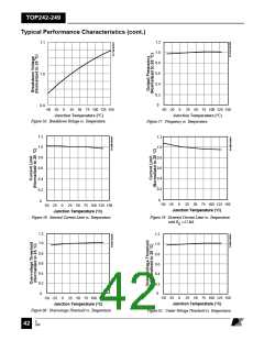
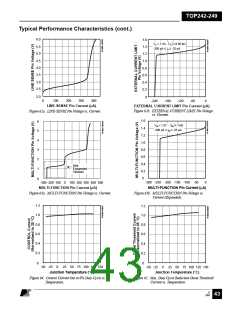
C. For externally adjusted current limit values, please refer to Figure 55 (Current Limit vs. External Current Limit
Resistance) in the Typical Performance Characteristics section.
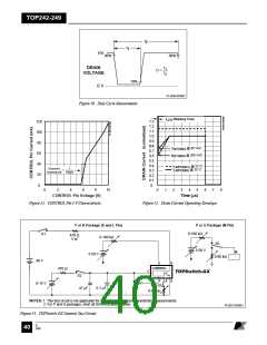
D. It is possible to start up and operate TOPSwitch-GX at DRAIN voltages well below 36 V. However, the
CONTROL pin charging current is reduced, which affects start-up time, auto-restart frequency, and auto-restart
duty cycle. Refer to Figure 67, the characteristic graph on CONTROL pin charge current (IC) vs. DRAIN voltage
for low voltage operation characteristics.
E
7/01
August 8, 2000
39

 POWERINT [ Power Integrations ]