TOP242-249
AHighEfficiency,250W,250–380VDCInputPowerSupply
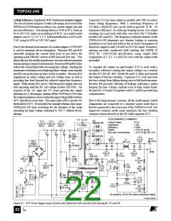
The circuit shown in figure 43 delivers 250 W (48 V @ 5.2 A)
at 84% efficiency using a TOP249 from a 250 to 380 VDC
input. DCinputisshown, astypicallyatthispowerlevelap.f.c.
boost stage would preceed this supply, providing the DC input
(C1 is included to provide local decoupling). Flyback topology
is still useable at this power level due to the high output voltage,
keeping the secondary peak currents low enough so that the
output diode and capacitors are reasonably sized.
is essential to limit the peak drain voltage during start-up and/
or overload conditions to below the 700 V rating of the
TOPSwitch-GX MOSFET.
The secondary is rectifed and smoothed by D2 and C9, C10 and
C11. Three capacitors are used to meet the secondary ripple
current requirement. Inductor L2 and C12 provide switching
noise filtering.
A simple Zener sensing chain regulates the output voltage. The
sum of the voltage drop of VR2, VR3 and VR4 plus the LED
drop of U2 gives the desired output voltage. Resistor R6 limits
LED current and sets overall control loop DC gain. Diode D4
and C14 provide secondary soft-finish, feeding current into the
CONTROLpinpriortooutputregulationandthusensuringthat
the output voltage reaches regulation at start-up under low line,
full load conditions. Resistor R9 provides a discharge path for
C14. CapacitorC13andR8providecontrolloopcompensation
and are required due to the gain associated with such a high
output voltage.
In this example the TOP249 is at the upper limit of its power
capability and the current limit is set to the internal maximum
by connecting the X pin to SOURCE. However, line sensing is
implemented by connecting a 2 MΩ resistor from the L pin to
the DC rail. If the DC input rail rises above 450 VDC, then
TOPSwitch-GX will stop switching until the voltage returns to
normal, preventing device damage.
Due to the high primary current, a low leakage inductance
transformer is essential. Therefore, a sandwich winding with a
copper foil secondary was used. Even with this technique the
leakage inductance energy is beyond the power capability of a
simple Zener clamp. Therefore, R2, R3 and C6 are added in
parallel to VR1. These have been sized such that during normal
operation very little power is dissipated by VR1, the leakage
energy instead being dissipated by R2 and R3. However, VR1
Sufficient heat sinking is required to keep the TOPSwitch-GX
device below 110 °C when operating under full load, low line
and maximum ambient temperature. Airflow may also be
required if a large heat sink area is not acceptable.
C7
2.2 nF Y1
D2
MUR1640CT
R2
R3
C6
C10
560 µF 560 µF
63 V 63 V
C11
L2
3 µH 8A
VR1
P6KE200
68 kΩ 68 kΩ 4.7 nF
48 V @ 5.2 A
+250 - 380 VDC
2 W
2 W
1 kV
C9
C12
560 µF
68 µF
63 V
63 V
D1
BYV26C
RTN
D2
1N4148
U2
LTV817A
R1
2 MΩ
1/2 W
R9
T1
C4
10 kΩ
1 µF
C1
50 V
22 µF
R6
400 V
100 Ω
TOPSwitch-GX
C13
150 nF
63 V
VR2 22 V
BZX79B22
D
S
L
TOP249Y
U1
D4
PERFORMANCE SUMMARY
1N4148
CONTROL
C
Output Power:
Line Regulation:
Load Regulation:
Efficiency:
250 W
1%
R4
5%
C14
22 µF
63 V
X
F
6.8 Ω
≥ 85%
VR3 12 V
BZX79B12
C3
R8
56 Ω
Ripple:
< 100 mV pk-pk
C3
0.1 µF
No Load Consumption: ≤ 1.4 W (300 VDC)
47 µF
50 V
VR4 12 V
BZX79B12
10 V
0V
All resistor 1/8 W 5% unless
otherwise stated.
PI-2692-033001
Figure 43. 250 W, 48 V Power Supply using TOP249.
E
7/01
August 8, 2000
23

 POWERINT [ Power Integrations ]