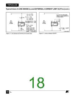
TOP242-249
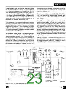
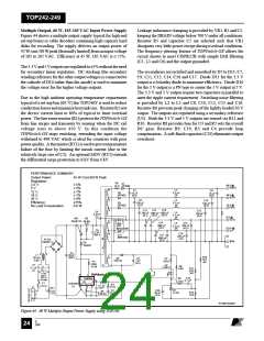
margin under worst case conditions. Resistor R4 provides line
sensing, setting UV at 100 VDC and OV at 450 VDC. The
extended maximum duty cycle feature of TOPSwitch-GX
(guaranteedminimumvalueof75%vs. 64%forTOPSwitch-II)
allows the use of a smaller input capacitor (C1). The extended
maximum duty cycle and the higher reflected voltage possible
with the RCD clamp also permit the use of a higher primary to
secondary turns ratio for T1 which reduces the peak reverse
voltage experienced by the secondary rectifier D8. As a result
a 60 V Schottky rectifier can be used for up to 15 V outputs,
whichgreatlyimprovespowersupplyefficiency. Thefrequency
reduction feature of the TOPSwitch-GX eliminates the need for
any dummy loading for regulation at no load and reduces the no
load/standby consumption of the power supply. Frequency
jitterprovidesimprovedmarginforconductedEMImeetingthe
CISPR 22 (FCC B) specification.
Application Examples
A High Efficiency, 30 W, Universal Input Power Supply
ThecircuitshowninFigure41takesadvantageofseveralofthe
TOPSwitch-GX features to reduce system cost and power
supply size and to improve efficiency. This design delivers
30 W at 12 V, from an 85 to 265 VAC input, at an ambient of
50 °C, in an open frame configuration. A nominal efficiency of
80% at full load is achieved using TOP244Y.
The current limit is externally set by resistors R1 and R2 to a
value just above the low line operating peak DRAIN current of
approximately70%ofthedefaultcurrentlimit. Thisallowsuse
of a smaller transformer core size and/or higher transformer
primary inductance for a given output power, reducing
TOPSwitch-GX power dissipation, while at the same time
avoiding transformer core saturation during startup and output
transient conditions. The resistors R1 & R2 provide a signal
that reduces the current limit with increasing line voltage,
which in turn limits the maximum overload power at high input
line voltage. This function in combination with the built-in
soft-startfeatureofTOPSwitch-GX,allowstheuseofalowcost
RCD clamp (R3, C3 and D1) with a higher reflected voltage, by
safelylimitingtheTOPSwitch-GXdrainvoltage, withadequate
Output regulation is achieved by using a simple Zener sense
circuit for low cost. The output voltage is determined by the
Zener diode (VR2) voltage and the voltage drops across the
optocoupler (U2) LED and resistor R6. Resistor R8 provides
bias current to Zener VR2 for typical regulation of 5% at the
12 V output level, over line and load and component variations.
PERFORMANCE SUMMARY
Output Power:
Regulation:
Efficiency:
Ripple:
30 W
4%
≥ 79%
≤ 50 mV pk-pk
CY1
2.2 nF
C14 R15
1 nF 150 Ω
L3
3.3 µH
12 V
@ 2.5 A
R3
C3
4.7 nF
1 kV
68 kΩ
C12
220 µF
35 V
D8
MBR1060
C10
560 µF
35 V
C11
560 µF
35 V
2 W
BR1
600 V
2A
D1
UF4005
RTN
D2
1N4148
R4
2 MΩ
R6
150 Ω
L1
20 mH
1/2 W
R8
R1
C6
0.1 µF
150 Ω
T1
4.7 MΩ
C1
1/2 W
U2
LTV817A
CX1
100 nF
250 VAC
68 µF
D
L
TOPSwitch-GX
400 V
U1
TOP244Y
CONTROL
C
R5
6.8 Ω
S
X
F
F1
3.15 A
VR2
1N5240C
10 V, 2%
J1
R2
9.09 kΩ
L
C5
47 µF
10 V
N
PI-2657-040501
Figure 41. 30 W Power Supply using External Current Limit Programming and Line Sensing for UV and OV.
E
7/01
August 8, 2000
21

 POWERINT [ Power Integrations ]