LNK302/304-306
be included for better EMI performance and higher line surge
withstand capability.
worst-case conditions of highest line voltage, maximum
overload (just prior to auto-restart) and highest ambient
temperature.
Quick Design Checklist
4) Thermal check – at maximum output power, minimum
input voltage and maximum ambient temperature, verify
that the LinkSwitch-TN SOURCE pin temperature is
100 °C or below. This figure ensures adequate margin due
to variations in RDS(ON) from part to part. Abattery powered
thermocouplemeterisrecommendedtomakemeasurements
whentheSOURCEpinsareaswitchingnode.Alternatively,
the ambient temperature may be raised to indicate margin
to thermal shutdown.
As with any power supply design, all LinkSwitch-TN designs
should be verified for proper functionality on the bench. The
following minimum tests are recommended:
1) Adequate DC rail voltage – check that the minimum DC
inputvoltagedoesnotfallbelow70VDCatmaximumload,
minimum input voltage.
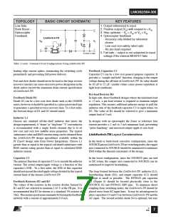
2) Correct Diode Selection – UF400x series diodes are
recommended only for designs that operate in MDCM at
an ambient of 70 °C or below. For designs operating in
continuousconductionmode(CCM)and/orhigherambients,
then a diode with a reverse recovery time of 35 ns or better,
such as the BYV26C, is recommended.
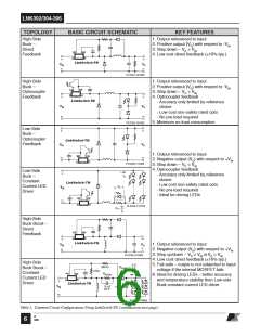
InaLinkSwitch-TNdesignusingabuckorbuckboostconverter
topology, the SOURCE pin is a switching node. Oscilloscope
measurements should therefore be made with probe grounded
to a DC voltage, such as primary return or DC input rail, and
not to the SOURCE pins. The power supply input must always
be supplied from an isolated source (e.g. via an isolation
transformer).
3) Maximum drain current – verify that the peak drain current
is below the data sheet peak drain specification under
G
8
3/05

 POWERINT [ Power Integrations ]