LNK302/304-306
KEY FEATURES
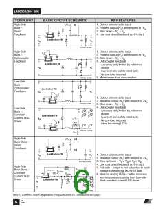
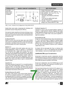
TOPOLOGY
BASIC CIRCUIT SCHEMATIC
Low-Side
1. Output referenced to input
2. Positive output (VO) with respect to +VIN
3. Step up/down – VO > VIN or VO < VIN
4. Optocoupler feedback
Buck Boost –
Optocoupler
Feedback
+
LinkSwitch-TN
- Accuracy only limited by reference
choice
VIN
VO
- Low cost non-safety rated opto
- No pre-load required
5. Fail-safe – output is not subjected to input
voltage if the internal MOSFET fails
BP
FB
+
D
S
PI-3756-111903
Table 2 (cont). Common Circuit Configurations Using LinkSwitch-TN.
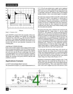
leading edge current spikes, terminating the switching cycle
prematurely and preventing full power delivery.
Feedback Capacitor C3
Capacitor C3 can be a low cost general purpose capacitor. It
provides a “sample and hold” function, charging to the output
voltage during the off time of LinkSwitch-TN. Its value should
be 10 µF to 22 µF; smaller values cause poorer regulation at
light load conditions.
Fast and slow diodes should never be used as the large reverse
recovery currents can cause excessive power dissipation in the
diode and/or exceed the maximum drain current specification
of LinkSwitch-TN.
Pre-load Resistor R4
Feedback Diode D2
In high-side, direct feedback designs where the minimum load
is <3 mA, a pre-load resistor is required to maintain output
regulation. This ensures sufficient inductor energy to pull the
inductor side of the feedback capacitor C3 to input return via
D2. The value of R4 should be selected to give a minimum
output load of 3 mA.
Diode D2 can be a low-cost slow diode such as the 1N400X
series, however it should be specified as a glass passivated type
to guarantee a specified reverse recovery time. To a first order,
the forward drops of D1 and D2 should match.
Inductor L1
Choose any standard off-the-shelf inductor that meets the
design requirements.A“drum” or “dog bone” “I” core inductor
is recommended with a single ferrite element due to to its
low cost and very low audible noise properties. The typical
inductance value and RMS current rating can be obtained from
the LinkSwitch-TN design spreadsheet available within the
PI Expert design suite from Power Integrations. Choose L1
greater than or equal to the typical calculated inductance with
RMS current rating greater than or equal to calculated RMS
inductor current.
In designs with an optocoupler the Zener or reference bias
current provides a 1 mA to 2 mA minimum load, preventing
“pulse bunching” and increased output ripple at zero load.
LinkSwitch-TN Layout Considerations
In the buck or buck-boost converter configuration, since the
SOURCEpinsinLinkSwitch-TNareswitchingnodes,thecopper
area connected to SOURCE should be minimized to minimize
EMI within the thermal constraints of the design.
Capacitor C2
In the boost configuration, since the SOURCE pins are tied
to DC return, the copper area connected to SOURCE can be
maximized to improve heatsinking.
The primary function of capacitor C2 is to smooth the inductor
current. The actual output ripple voltage is a function of this
capacitorʼs ESR. To a first order, the ESR of this capacitor
shouldnotexceedtheratedripplevoltagedividedbythetypical
current limit of the chosen LinkSwitch-TN.
The loop formed between the LinkSwitch-TN, inductor (L1),
freewheeling diode (D1), and output capacitor (C2) should
be kept as small as possible. The BYPASS pin capacitor
C1 (Figure 6) should be located physically close to the
SOURCE (S) and BYPASS (BP) pins. To minimize direct
coupling from switching nodes, the LinkSwitch-TN should be
placed away from AC input lines. It may be advantageous to
place capacitors C4 and C5 in-between LinkSwitch-TN and the
AC input. The second rectifier diode D4 is optional, but may
Feedback Resistors R1 and R3
The values of the resistors in the resistor divider formed by
R1 and R3 are selected to maintain 1.65 V at the FB pin. It is
recommended that R3 be chosen as a standard 1% resistor of
2kΩ. Thisensuresgoodnoiseimmunitybybiasingthefeedback
network with a current of approximately 0.8 mA.
G
3/05
7

 POWERINT [ Power Integrations ]