LNK302/304-306
LinkSwitch-TN
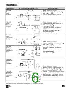
RF1
D1
L2
D
FB
BP
S
D2
R1
+
C1
AC
INPUT
S
S
L1
C4
C5
C3
R3
DC
OUTPUT
C2
S
D1
D4
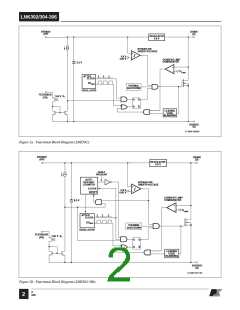
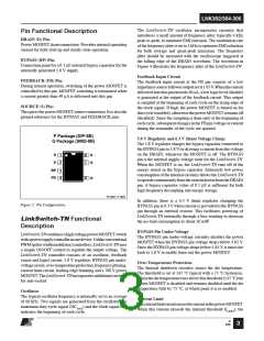
Optimize hatched copper areas (
) for heatsinking and EMI.
PI-3750-083004
Figure 6. Recommended Printed Circuit Layout for LinkSwitch-TN in a Buck Converter Configuration.
cycles are skipped. To provide overload protection if no cycles
LinkSwitch-TN Selection and Selection Between
are skipped during a 50 ms period, LinkSwitch-TN will enter
auto-restart (LNK304-306), limiting the average output power
to approximately 6% of the maximum overload power. Due to
trackingerrorsbetweentheoutputvoltageandthevoltageacross
C3 at light load or no load, a small pre-load may be required
(R4). For the design in Figure 5, if regulation to zero load is
required, then this value should be reduced to 2.4 kΩ.
MDCM and CCM Operation
SelecttheLinkSwitch-TNdevice,freewheelingdiodeandoutput
inductor that gives the lowest overall cost. In general, MDCM
provides the lowest cost and highest efficiency converter. CCM
designs require a larger inductor and ultra-fast (trr ≤35 ns)
freewheeling diode in all cases. It is lower cost to use a larger
LinkSwitch-TNinMDCMthanasmallerLinkSwitch-TNinCCM
because of the additional external component costs of a CCM
design. However, ifthehighestoutputcurrentisrequired, CCM
should be employed following the guidelines below.
Key Application Considerations
LinkSwitch-TN Design Considerations
Output Current Table
Topology Options
Data sheet maximum output current table (Table 1) represents
the maximum practical continuous output current for both
mostlydiscontinuousconductionmode(MDCM)andcontinuous
conductionmode(CCM)ofoperationthatcanbedeliveredfrom
a given LinkSwitch-TN device under the following assumed
conditions:
LinkSwitch-TN can be used in all common topologies, with or
withoutanoptocouplerandreferencetoimproveoutputvoltage
tolerance and regulation. Table 2 provide a summary of these
configurations. For more information see the Application
Note – LinkSwitch-TN Design Guide.
1) Buck converter topology.
Component Selection
2) The minimum DC input voltage is ≥70 V. The value of
input capacitance should be large enough to meet this
criterion.
3) For CCM operation a KRP* of 0.4.
4) Output voltage of 12 VDC.
Referring to Figure 5, the following considerations may be
helpful in selecting components for a LinkSwitch-TN design.
Freewheeling Diode D1
5) Efficiency of 75%.
Diode D1 should be an ultra-fast type. For MDCM, reverse
recovery time trr ≤75 ns should be used at a temperature of
70°Corbelow. Slowerdiodesarenotacceptable,ascontinuous
mode operation will always occur during startup, causing high
leading edge current spikes, terminating the switching cycle
prematurely,andpreventingtheoutputfromreachingregulation.
If the ambient temperature is above 70 °C then a diode with
trr ≤35 ns should be used.
6) A catch/freewheeling diode with trr ≤75 ns is used for
MDCM operation and for CCM operation, a diode with
trr ≤35 ns is used.
7) The part is board mounted with SOURCE pins soldered
to a sufficient area of copper to keep the SOURCE pin
temperature at or below 100 °C.
*KRP is the ratio of ripple to peak inductor current.
For CCM an ultra-fast diode with reverse recovery time
trr ≤35 ns should be used. A slower diode may cause excessive
G
3/05
5

 POWERINT [ Power Integrations ]