RELEASED
PM7350 S/UNI DUPLEX
DATA SHEET
PMC-1980581
ISSUE 8
DUAL SERIAL LINK PHY MULTIPLEXER
SCI-PHY/Utopia16-bit master:
SCI-PHY/Utopia16-bit slave:
Any-PHY 16-bit slave:
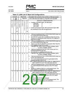
54B (base cell + UDF)
54B (base cell + UDF)
56B (base cell + UDF + 2 address)
The similar output port default configuration produces the following cell
lengths:
SCI-PHY/Utopia 8-bit master:
SCI-PHY 8-bit slave:
Any-PHY 8-bit slave:
SCI-PHY/Utopia16-bit master
SCI-PHY16-bit slave:
Any-PHY16-bit slave:
53B
54B (base cell + address)
54B (base cell + address)
54B (base cell + UDF)
56B (base cell + 2 address)
56B (base cell + UDF + 2 address)
In Table 19 to Table 23, these would be referred as 53/53/54(54/54/56) and
53/54/54(54/54/56) byte bus length.
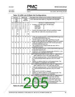
• When the input side is configured as a 8-bit parallel bus or as a clocked serial
data interface and the output side is configured as a 16-bit parallel bus, the
UDF is undefined at the far end independently of the LVDS link configuration.
When the input side is configured as a 16-bit parallel bus and the output side
is configured as a 8-bit parallel bus or as a clocked serial data interface, the
UDF is stripped at the far end.
• When using the CSD (Clock Serial Data interface), the cell size is fixed at 53
bytes. By default, cell delineation is enable on the Clocked Serial Data receive
port (Receive Serial Indirect Channel Configuration register 0x69,
DDELIN=0). The HCS value is used only to acquire and maintain cell
delineation and does not need to be carried to the other side. Similarly, by
default the HCS value is generated by the Clock Serial Data transmit interface
(Transmit Serial Indirect Channel Data register 0x71, DHCS=0) and does
need to be carried over the LVDS link.
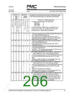
• When unframed data is transported through the Clocked Serial Data interface,
data is packet in 53 byte packet and carried transparently. All five fields of the
cell header are used and must be carried.
• For control cells written or read via the microprocessor port, bytes 0&1
correspond to the microprocessor port’s unique PHY address field. However
since this field is fixed there is no useful information in these bytes. Bytes
10&11 are always undefined. Bytes 2&3 correspond to the user prepend
bytes, and bytes 8&9 correspond to the H5&HDF bytes.
• The PHY address field is transported across the LVDS in an extra word added
to each user cell. Therefore it is not necessary that the H5 (H5/UDF) field be
sent over the LVDS link even if the output bus interfaces is configured to
embed the PHY address in the H5 (H5/UDF) field. This will slightly
increase the effective throughput of the LVDS, but it will impact control cells
PROPRIETARY AND CONFIDENTIAL TO PMC-SIERRA, INC., AND FOR ITS CUSTOMERS’ INTERNAL USE
188

 PMC [ PMC-SIERRA, INC ]