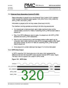
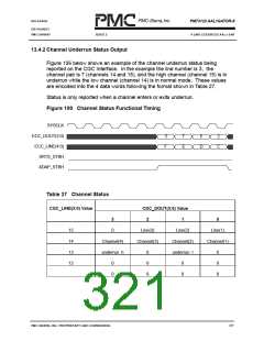
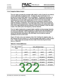
RELEASED
PM73123 AAL1GATOR-8
DATASHEET
PMC-2000097
ISSUE 2
8 LINK CES/DBCES AAL1 SAR
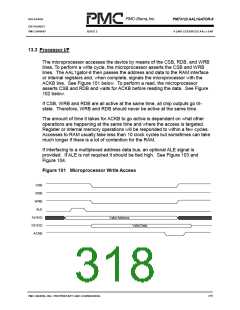
13.3 Processor I/F
The microprocessor accesses the device by means of the CSB, RDB, and WRB
lines. To perform a write cycle, the microprocessor asserts the CSB and WRB
lines. The AAL1gator-8 then passes the address and data to the RAM interface
or internal registers and, when complete, signals the microprocessor with the
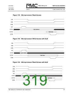
ACKB line. See Figure 101 below. To perform a read, the microprocessor
asserts CSB and RDB and waits for ACKB before reading the data. See Figure
102 below.
If CSB, WRB and RDB are all active at the same time, all chip outputs go tri-
state. Therefore, WRB and RDB should never be active at the same time.
The amount of time it takes for ACKB to go active is dependant on what other
operations are happening at the same time and where the access is targeted.
Register or internal memory operations will be responded to within a few cycles.
Accesses to RAM usually take less than 10 clock cycles but sometimes can take
much longer if there is a lot of contention for the RAM.
If interfacing to a multiplexed address data bus, an optional ALE signal is
provided. If ALE is not required it should be tied high. See Figure 103 and
Figure 104.
Figure 101 Microprocessor Write Access
CSB
RDB
WRB
ALE
A(19:0)
D(15:0)
ACKB
Valid Address
Valid Data
PMC-SIERRA, INC. PROPRIETARY AND CONFIDENTIAL
318

 PMC [ PMC-SIERRA, INC ]