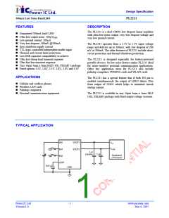
Design Specification
300mA Low Noise Dual LDO
PL2211
rising time is 35us typically at 300mA output current.
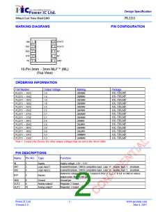
Connect EN pin to IN pin for normal operation
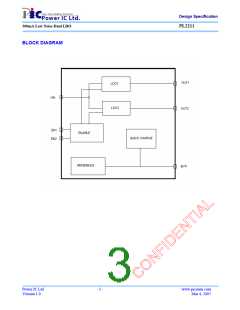
OPERATION DESCRIPTION
The PL2211 are ultra-low-noise, low-dropout, low-
quiescent current linear regulators designed for space-
restricted applications. These devices can supply loads up
to 300mA. As shown in the Block Diagram, the PL2211
consists of a highly accurate band gap core, noise bypass
circuit, error amplifier, P-channel pass transistor and an
internal feedback voltage divider. The 1.0V band gap
reference is connected to the error amplifier’s inverting
input. The error amplifier compares this reference with
the feedback voltage and amplifies the difference. If the
feedback voltage is lower than the reference voltage, the
pass transistor gate is pulled low. This allows more
current to pass to the output and increases the output
voltage. If the feedback voltage is too high, the pass
transistor gate is pulled high, allowing less current to
pass to the output. The output voltage is feedback
through an internal resistor voltage divider connected to
the OUT pin. An external bypass capacitor connected to
BYP reduces noise at the output. Additional blocks
include a current limiter, over temperature protection,
and shutdown logic.
Under Voltage Lockout
When the input supply goes too low (below 2.0V) the
PL2211 produces an internal UVLO (under voltage
lockout) signal that generates a fault signal and shuts
down the chip. This mechanism protects the chip from
producing false logic due to low input supply.
Quick Charging Mode
The PL2211 has a quick charge block to get the reference
up very quickly by charging the BYP capacitor with very
high current when the chip comes out of shut down. This
quick charge block stops charging the BYP capacitor
when the reference reaches 95% of its nominal value and
then the chip switches out of quick charging mode to
normal operating mode.
Over Temperature Protection
Over temperature protection limits total power
dissipation in the PL2211. When the junction
temperature exceeds Tj= +155°C, the thermal sensor
signals the shutdown logic and turns off the pass
transistor. The thermal sensor turns the pass transistor on
again after the IC’s junction temperature drops by 15°C,
resulting in a pulsed output during continuous thermal-
overload conditions.
Internal P-Channel Pass Transistor
The PL2211 feature a 1Ω (typ) P-channel MOSFET pass
transistor. This provides several advantages over similar
designs using a PNP pass transistor, including longer
battery life. The P-channel MOSFET requires no base
drive, which considerably reduces quiescent current.
PNP-based regulators waste considerable current in
dropout when the pass transistor saturates. They also use
high base-drive current under heavy loads. The PL2211
does not suffer from these problems and consume only
200µA of quiescent current in light load.
Thermal-Overload protection is design to protect the
PL2211 in the event of a fault condition. For continual
operation, do not exceed the absolute maximum junction
temperature rating of Tj = +150°C.
Current Limit
Operating Region and Power Dissipation
The PL2211 includes a current limiter. It monitors the
output current and controls the pass transistor’s gate
voltage to limit the output current under 550mA (typ).
The output can be shorted to ground for an indefinite
amount of time without damaging the part.
The PL2211 maximum power dissipation depends on 1)
the thermal resistance of the case and circuit board, 2) the
temperature difference between the die junction and
ambient, and 3) the rate of airflow. The power dissipation
across the device is:
Enable Input
P = Iout ( Vin – Vout )
The maximum power dissipation is:
Pmax = (Tj – Ta) / (θjc + θca)
The PL2211 features an active-high Enable input (EN)
pin that allows on/off control of the regulator. The
PL2211 bias current reduces to less than microampere of
leakage current when it is shutdown. The Enable input is
TTL/CMOS compatible threshold for simple logic
interfacing. When EN is ‘H,’ the output voltage startup
Where (Tj – Ta) is the temperature difference between
the PL2211 die junction and the ambient air; θjc is the
thermal resistance of the package; and θca is the thermal
Power IC Ltd.
Version 1.0
- 5 -
www.picsemi.com
Mar 4, 2007

 PICSEMI [ POWER IC LTD. ]