Design Specification
300mA Low Noise Dual LDO
PL2211
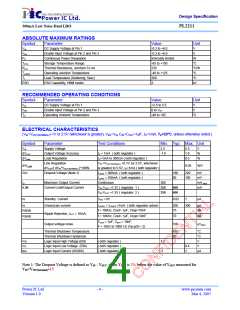
ABSOLUTE MAXIMUM RATINGS
Symbol
Parameter
Value
Unit
V
VIN
DC Supply Voltage at Pin 1
-0.3 to +6.0
-0.3 to +6.0
Internally limited
-65 to +150
235
VEN
Enable Input Voltage at Pin 2 and Pin 3
Continuous Power Dissipation
Storage Temperature Range
Thermal Resistance, Junction-To-Air
Operating Junction Temperature
Lead Temperature (Soldering, 5sec)
ESD Capability, HBM model
V
PD
W
TSTG
RθJA
TJ,MAX
TL
℃
℃/W
℃
℃
kV
-40 to +125
260
ESD
2
RECOMMENDED OPERATING CONDITIONS
Symbol
Parameter
Value
+2.5 to 5.5
Unit
V
VIN
DC Supply Voltage at Pin 1
Enable Input Voltage at Pin 2 and Pin 3
Operating Ambient Temperature
VEN
0 to VIN
V
TA
-40 to +85
℃
ELECTRICAL CHARACTERISTICS
(VIN=VOUT(NOMINAL)+1V or 2.5V (whichever is greater), VEN=VIN, CIN=COUT=1µF, IO=1mA, TA=25°C, unless otherwise noted.)
Symbol
VIN
Parameter
Supply Voltage
Test Conditions
Min. Typ. Max. Unit
2.5
5.5
1.0
0.5
V
∆VOUT
∆Vload
Output Voltage Accuracy
Load Regulation
IO = 1mA ( both regulator )
-1.0
%
%
IO=1mA to 300mA ( both regulator )
Line Regulation
VIN =VOUT(NOMINAL) +0.1V (or 2.5V, whichever
∆Vl LINE
0.05
%/V
dVOUT/( dVIN*VOUT(NOMINAL) )*100%
Dropout Voltage (Note 1)
is greater) to 5.5V, IO=1mA ( both regulator )
ILOAD = 300mA ( both regulator )
ILOAD = 100mA ( both regulator )
Continuous
VDP
180
80
220
100
mV
mV
IO
Maximum Output Current
300
350
350
mA RMS
mA
ILIM
Current Limit/Output Current
VIN-VOUT =1.3V ( regulator 1 )
VIN-VOUT =1.3V ( regulator 2 )
600
600
IQ
Standby Current
VEN = 0V
0.02
1
µA
IG
Ground pin current
ILOAD1 = ILOAD2 =1mA ( both regulator active)
f = 100Hz, Cout= 1µF, Cbyp=10nF
200
75
300
µA
dB
PSRR
PSRR
Ripple Rejection, IOUT = 10mA,
Output voltage noise
f = 10KHz, Cout= 1µF, Cbyp=10nF
70
dB
COUT = 1µF, CBYP = 10nF,
100
µVRMS
F = 10Hz to 100K Hz (Vp-p/2/√ 2)
Thermal Shutdown Temperature
Thermal Shutdown Hysteresis
Logic Input High Voltage (EN)
Logic Input Low Voltage (EN\)
Logic Input Current (SHDN\)
165
20
°C
°C
V
VIH
VIL
IEN
( both regulator )
( both regulator )
( both regulator )
1.2
-1
0.4
1
V
µA
Note 1: The Dropout Voltage is defined as VIN - VOUT, when VOUT is 2% below the value of VOUT measured for
VIN=VOUT(nominal)+1V.
Power IC Ltd.
Version 1.0
- 4 -
www.picsemi.com
Mar 4, 2007

 PICSEMI [ POWER IC LTD. ]