Design Specification
300mA Low Noise Dual LDO
PL2211
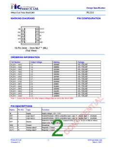
MARKING DIAGRAMS
PIN CONFIGURATION
ORDERING INFORMATION
Part Number
Output Voltage
Marking
DBAMW
DBBMW
DBCMW
DBDMW
DBEMW
DBFMW
DBGMW
DBHMW
DBIMW
Package
10L-TDLMF
10L-TDLMF
10L-TDLMF
10L-TDLMF
10L-TDLMF
10L-TDLMF
10L-TDLMF
10L-TDLMF
10L-TDLMF
10L-TDLMF
10L-TDLMF
10L-TDLMF
10L-TDLMF
10L-TDLMF
PL2211 – 15VZ
PL2211 – 15UZ
PL2211 – 18VZ
PL2211 – 18UZ
PL2211 – 25VZ
PL2211 – 25UZ
PL2211 – 27VZ
PL2211 – 27UZ
PL2211 – 28VZ
PL2211 – 28UZ
PL2211 – 30VZ
PL2211 – 30UZ
PL2211 – 33VZ
PL2211 – 33UZ
1.5
1.5
1.8
1.8
2.5
2.5
2.7
2.7
2.8
2.8
3.0
3.0
3.3
3.3
DBJMW
DBKMW
DBLMW
DBMMW
DBNMW
Note 1: Contact the factory for other output voltages that are not in the above table
PIN DESCRIPTIONS
Name
Pin NO. Type
Function
IN
1
2
3
Supply
Supply voltage. 2.5V ~ 5.5V.
EN1
EN2
Logic input 1
Logic input 2
Enable/Shutdown. CMOS compatible input. Logic ‘H’ : enable, logic ‘L’ : shutdown.
Enable/Shutdown. CMOS compatible input. Logic ‘H’ : enable, logic ‘L’ : shutdown.
Reference voltage bypass pin. Connect 0.01uF ≦ CBYP ≦ 0.1uF to GND to reduce
output noise. May be left open.
BYP
4
Bypass
GND
6
Ground
Ground pin
OUT2
OUT1
9
Analog output2
Analog output1
Regulator 2 Output.
Regulator 1 Output.
10
Power IC Ltd.
Version 1.0
- 2 -
www.picsemi.com
Mar 4, 2007

 PICSEMI [ POWER IC LTD. ]