Philips Semiconductors
Preliminary specification
Economy audio CODEC for MiniDisc (MD)
home stereo and portable applications
UDA1341TS
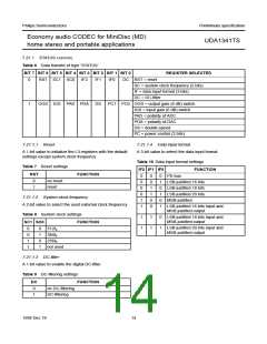
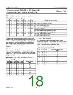
7.21.1 STATUS CONTROL
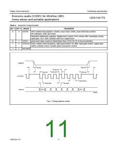
Table 6 Data transfer of type ‘STATUS’
BIT 7 BIT 6 BIT 5 BIT 4 BIT 3 BIT 2 BIT 1 BIT 0
REGISTER SELECTED
0
1
RST SC1 SC0
IF2
IF1
IF0
DC RST = reset
SC = system clock frequency (2 bits)
IF = data input format (3 bits)
DC = DC-filter
OGS IGS PAD PDA
DS
PC1 PC0 OGS = output gain (6 dB) switch
IGS = input gain (6 dB) switch
PAD = polarity of ADC
PDA = polarity of DAC
DS = double speed
PC = power control (2 bits)
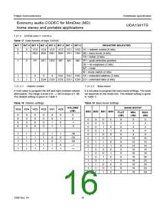
7.21.1.1 Reset
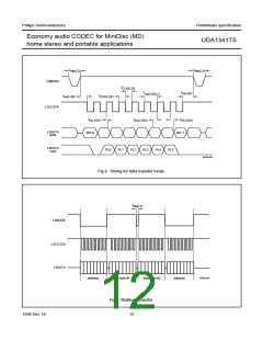
7.21.1.4 Data input format
A 1-bit value to initialize the L3-registers with the default
settings except system clock frequency.
A 3-bit value to select the data input format.
Table 10 Data input format settings
Table 7 Reset settings
IF2 IF1 IF0
FUNCTION
RST
FUNCTION
0
0
0
0
1
1
0
0
1
1
0
0
0
1
0
1
0
1
I2S-bus
0
1
no reset
reset
LSB-justified 16 bits
LSB-justified 18 bits
LSB-justified 20 bits
MSB-justified
7.21.1.2 System clock frequency
A 2-bit value to select the used external clock frequency.
LSB-justified 16 bits input and
MSB-justified output
Table 8 System clock settings
1
1
1
1
0
1
LSB-justified 18 bits input and
MSB-justified output
SC1 SC0
FUNCTION
LSB-justified 20 bits input and
MSB-justified output
0
0
1
1
0
1
0
1
512fs
384fs
256fs
not used
7.21.1.3 DC-filter
A 1-bit value to enable the digital DC-filter.
Table 9 DC-filtering settings
DC
FUNCTION
0
1
no DC-filtering
DC-filtering
1998 Dec 18
14

 NXP [ NXP ]