Philips Semiconductors
Product specification
High speed CAN transceiver
TJA1041A
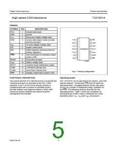
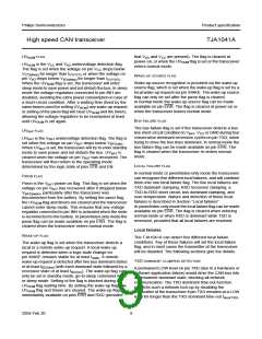
PINNING
SYMBOL PIN
DESCRIPTION
transmit data input
TXD
GND
VCC
1
2
3
4
ground
transceiver supply voltage input
handbook, halfpage
TXD
1
2
3
4
5
6
7
14 STB
RXD
receive data output; reads out data
from the bus lines
GND
13 CANH
12 CANL
11 SPLIT
VI/O
EN
5
6
7
I/O-level adapter voltage input
enable control input
V
CC
RXD
TJA1041AT
INH
inhibit output for switching external
voltage regulators
V
10
9
V
BAT
I/O
ERR
8
error and power-on indication output
(active LOW)
WAKE
ERR
EN
INH
8
WAKE
VBAT
9
local wake-up input
MDB635
10 battery voltage input
SPLIT
CANL
CANH
STB
11 common-mode stabilization output
12 LOW-level CAN bus line
13 HIGH-level CAN bus line
14 standby control input (active LOW)
Fig.2 Pinning configuration.
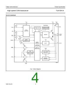
FUNCTIONAL DESCRIPTION
Operating modes
The primary function of a CAN transceiver is to provide the
CAN physical layer as described in the ISO 11898
standard. In the TJA1041A this primary function is
complemented with a number of operating modes,
fail-safe features and diagnosis features, which offer
enhanced system reliability and advanced power
management functionality.
The TJA1041A can be operated in five modes, each with
specific features. Control pins STB and EN select the
operating mode. Changing between modes also gives
access to a number of diagnostics flags, available via
pin ERR. The following sections describe the five
operating modes. Table 1 shows the conditions for
selecting these modes. Figure 3 illustrates the mode
transitions when VCC, VI/O and VBAT are present.
2004 Feb 20
5

 NXP [ NXP ]