Philips Semiconductors
Product specification
New In Car Entertainment car radio tuner IC with
Precision Adjacent Channel Suppression (NICE-PACS)
TEA6848H
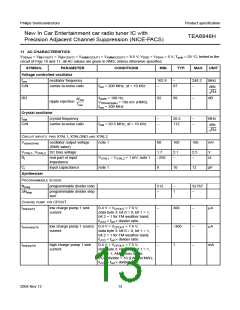
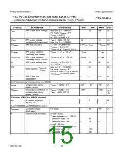
7.6
IF2 filter gain alignment
7.7
Frequency offset detector/alignment
The 4-bit filter gain alignment reduces the change in
IF filter gain spread when the bandwidth is changed in
dynamic mode from 155 kHz (maximum) to 25 kHz
(minimum).
A very strong undesired neighbouring signal causes offset
in the demodulator in case of weak desired input signal.
The frequency offset detector reduces the bandwidth of
the IF2 filter when the detected offset in the demodulator
is too large.
A frequency has to be chosen in the middle of
European/US FM band, Japan band or OIRT band (for
East Europe) and the IC has to be set into dynamic
bandwidth mode (IF2 bandwidth is 155 kHz).
There are four bits available for frequency offset detector
alignment. Every band has to be aligned separately.
Tuning has to be set to middle of the band, input signal
unmodulated, bit IFBW = 1 (alignment voltage will be
given to pin IFBWFLAG). The DC voltage at
Setting and clearing the FMBW bit continuously allows the
adjustment of the gain alignment to minimum change in
AM/FM DC level.
pin IFBWFLAG has to be aligned to the minimum value.
8
LIMITING VALUES
In accordance with the Absolute Maximum Rating System (IEC 60134).
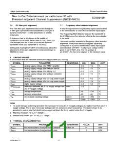
SYMBOL
VDDA1
PARAMETER
CONDITIONS
MIN.
−0.3
MAX.
+10
UNIT
analog supply voltage 1 for FM IF amplifier
analog supply voltage 2 for FM and AM RF
analog supply voltage 3 for tuning PLL
V
V
V
V
VDDA2
VDDA3
VDDA4
−0.3
−0.3
−0.3
+10
+10
+10
analog supply voltage 4 for voltage controlled
oscillator
VDDA5
analog supply voltage 5 for on-chip power supply
analog supply voltage 6 for on-chip power supply
digital supply voltage
−0.3
−0.3
−0.3
−0.3
+6.5
+10
+6.5
−
V
V
V
V
VDDA6
VDDD
∆VDD8.5-DD5
difference between any 8.5 V supply voltage and note 1
any 5 V supply voltage
Tstg
Tamb
Ves
storage temperature
ambient temperature
−55
+150
+85
°C
°C
V
−40
electrostatic handling voltage
note 2
note 3
−200
−2000
+200
+2000
V
Notes
1. To avoid damage and wrong operation it is necessary to keep all 8.5 V supply voltages at a higher level than any 5 V
supply voltage. This is also necessary during power-on and power-down sequences. Precautions have to be
provided in such a way that interference cannot pull down the 8.5 V supply below the 5 V supply.
2. Machine model (R = 0 Ω, C = 200 pF).
3. Human body model (R = 1.5 kΩ, C = 100 pF).
9
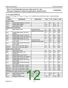
THERMAL CHARACTERISTICS
SYMBOL
Rth(j-a)
PARAMETER
CONDITIONS
VALUE
UNIT
thermal resistance from junction to ambient
thermal resistance from junction to case
in free air
54
9
K/W
K/W
Rth(j-c)
2004 Nov 12
11

 NXP [ NXP ]