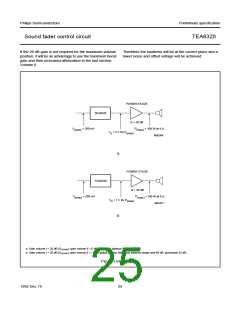
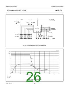
Philips Semiconductors
Preliminary specification
Sound fader control circuit
TEA6320
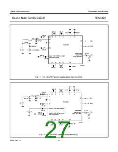
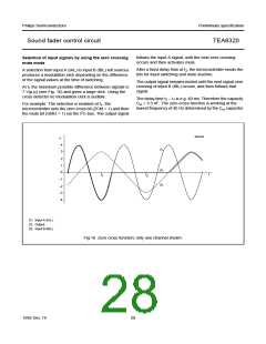
follows the input A signal, until the next zero crossing
occurs and then activates mute.
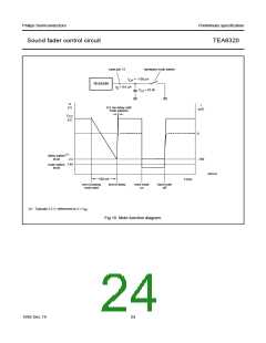
Selection of input signals by using the zero crossing
mute mode
After a fixed delay time at t2, the microcontroller sends the
bits for input switching and mute inactive.
A selection from input A (IAL) to input B (IBL) left sources
produces a modulation click depending on the difference
of the signal values at the time of switching.
The output signal remains muted until the next signal zero
crossing of input B (IBL) occurs, and then follows that
signal.
At t1 the maximum possible difference between signals is
7 V(p-p) (see Fig. 16) and gives a large click. Using the
cross detector no modulation click is audible.
The delay time t2 − t1 is e.g. 40 ms. Therefore the capacity
Cm = 3.3 nF. The zero cross function is working at the
lowest frequency of 40 Hz determined by the Cm capacitor.
For example: The selection is enabled at t1, the
microcontroller sets the zero cross bit (ZCM = 1) and then
the mute bit (GMU = 1) via the I2C-bus. The output signal
handbook, full pagewidth
V
MED436
4
3
(1)
2
1
0
(2)
t
t
t
2
1
−1
(3)
−2
−3
−4
(1) Input A (IAL).
(2) Output.
(3) Input B (IBL).
Fig.16 Zero cross function; only one channel shown.
1995 Dec 19
28

 NXP [ NXP ]