Philips Semiconductors
Preliminary specification
Sound fader control circuit
TEA6320
handbook, full pagewidth
220 nF
33 nF
5.6 nF
10 nF
100 µF
10
8
7
6
5
12
21
31
VCC = 8.5 V
0.1 µF
32
1
SCL
SDA
10 kΩ
2
TEA6320
1000 µF
19
VP
47 µF
0.2 V (RMS)
output right
output left
front and rear
4.7 µF
VO
600 Ω
input A to D left and right
and input mono
220 nF
23 25
220 nF
26 27
33 nF
28
MED434
5.6 nF
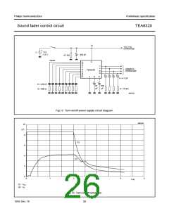
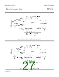
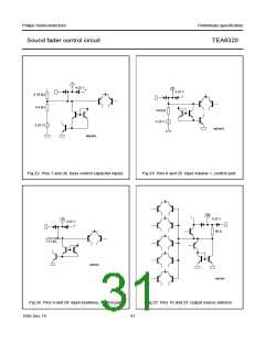
Fig.14 Test circuit for power supply ripple rejection (RR).
handbook, full pagewidth
220 nF
33 nF
5.6 nF
10 nF
100 µF
10
8
7
6
5
12
21
31
V
CC = 8.5 V
0.1 µF
32
1
SCL
470 µF
2
TEA6320
Vp
SDA
19
47 µF
input A to D right and left
220 nF
600 Ω
4.7 µF
output left
output right
front and rear
Vi
VO
input A to D left and right
and input mono
220 nF
23 25
220 nF
26 27
33 nF
28
MED435
5.6 nF
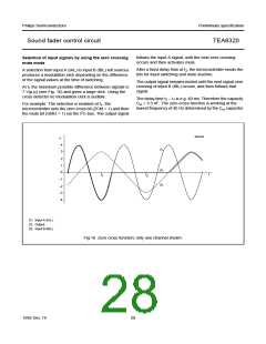
Fig.15 Test circuit for channel separation (αcs).
1995 Dec 19
27

 NXP [ NXP ]