TEA1532
Philips Semiconductors
GreenChip II SMPS control IC
– for packages with a thickness ≥ 2.5 mm
– for packages with a thickness < 2.5 mm and a volume ≥ 350 mm3 so called
thick/large packages.
• below 240 °C (SnPb process) or below 260 °C (Pb-free process) for packages with a
thickness < 2.5 mm and a volume < 350 mm3 so called small/thin packages.
Moisture sensitivity precautions, as indicated on packing, must be respected at all times.
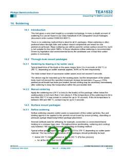
14.3.2 Wave soldering
Conventional single wave soldering is not recommended for surface mount devices
(SMDs) or printed-circuit boards with a high component density, as solder bridging and
non-wetting can present major problems.
To overcome these problems the double-wave soldering method was specifically
developed.
If wave soldering is used the following conditions must be observed for optimal results:
• Use a double-wave soldering method comprising a turbulent wave with high upward
pressure followed by a smooth laminar wave.
• For packages with leads on two sides and a pitch (e):
– larger than or equal to 1.27 mm, the footprint longitudinal axis is preferred to be
parallel to the transport direction of the printed-circuit board;
– smaller than 1.27 mm, the footprint longitudinal axis must be parallel to the
transport direction of the printed-circuit board.
The footprint must incorporate solder thieves at the downstream end.
• For packages with leads on four sides, the footprint must be placed at a 45° angle to
the transport direction of the printed-circuit board. The footprint must incorporate
solder thieves downstream and at the side corners.
During placement and before soldering, the package must be fixed with a droplet of
adhesive. The adhesive can be applied by screen printing, pin transfer or syringe
dispensing. The package can be soldered after the adhesive is cured.
Typical dwell time of the leads in the wave ranges from 3 to 4 seconds at 250 °C or
265 °C, depending on solder material applied, SnPb or Pb-free respectively.
A mildly-activated flux will eliminate the need for removal of corrosive residues in most
applications.
14.3.3 Manual soldering
Fix the component by first soldering two diagonally-opposite end leads. Use a low voltage
(24 V or less) soldering iron applied to the flat part of the lead. Contact time must be
limited to 10 seconds at up to 300 °C.
When using a dedicated tool, all other leads can be soldered in one operation within
2 to 5 seconds between 270 and 320 °C.
9397 750 13113
© Koninklijke Philips Electronics N.V. 2004. All rights reserved.
Preliminary data sheet
Rev. 01 — 28 May 2004
23 of 27

 NXP [ NXP ]