TEA1532
Philips Semiconductors
GreenChip II SMPS control IC
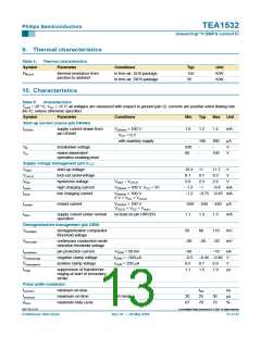
Table 5:
Characteristics …continued
Tamb = 25 °C; VCC = 15 V; all voltages are measured with respect to ground (pin 2); currents are positive when flowing into
the IC; unless otherwise specified.
Symbol
Oscillator
fosc
Parameter
Conditions
Min
Typ
Max
Unit
oscillator frequency (fixed
frequency)
VCTRL < 1 V
50
63
75
kHz
Duty cycle control (pin CTRL)
Vmin
minimum voltage for maximum
duty cycle
-
-
1.0
1.5
-
-
V
V
Vmax
maximum voltage for minimum
duty cycle
∆Islopecomp/∆t
slope compensation current
Control detect level
−1.2
−1
−0.8
µA/µs
VCTRL(detect)
0.56
0.63
0.70
V
Protection and timing input (pin PROTECT)
Vtrip
trip level
2.37
2.85
-
2.5
3
2.63
3.15
-
V
V
V
Vtrip(latch)
VCC(latch)(reset)
trip level for latch
voltage level on pin VCC which VCC(latch) < 2.3 V
resets the latch
4.5
Icharge
charge current
VCTRL < 0.63 V
−57
−50
−43
µA
Idischarge
discharge current
-
100
-
nA
Valley switch (pin DRAIN)
∆V/∆tvalley
valley recognition voltage
change
−43
-
+43
-
V/µs
[1]
tvalley-swon
delay from valley recognition to
switch-on
-
150
ns
Overcurrent and winding short-circuit protection (pin SENSE)
Vsense(max)
maximum source voltage for
OCP
∆V/∆t = 0.1 V/µs
0.48
-
0.52
140
0.56
185
V
tPD
propagation delay from
detecting Vsense(max) to
switch-off
∆V/∆t = 0.5 V/µs
ns
tleb
Iss
blanking time for current and
winding short-circuit protection
330
45
400
60
470
75
ns
soft start current
Vsense < 0.5 V
µA
Brown-out protection (pin DEM)
[2]
Ibrown-out
brown-out protection current
A constant I(brown-out) is drawn
from pin DEM.
−68
−60
−52
µA
µs
ton(min)(brown-out)
minimum on-time for enabling
the brown-out protection.
1.5
2
2.5
Driver (pin DRIVER)
Isource source current
Isink
VCC = 9.5 V; VDRIVER = 2 V
VCC = 9.5 V;
-
−170 −88
mA
sink current
VDRIVER = 2 V
-
300
700
11.5
-
mA
mA
V
VDRIVER = 9.5 V
VCC > 12 V
400
-
-
Vo(max)
maximum output voltage
12
9397 750 13113
© Koninklijke Philips Electronics N.V. 2004. All rights reserved.
Preliminary data sheet
Rev. 01 — 28 May 2004
14 of 27

 NXP [ NXP ]