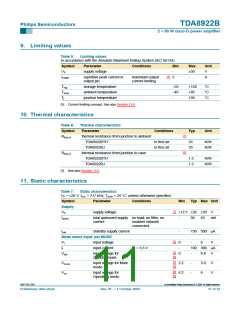
TDA8922B
Philips Semiconductors
2 × 50 W class-D power amplifier
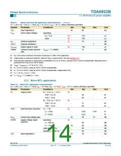
Table 10: Mono BTL application characteristics …continued
VP = ±26 V; RL = 8 Ω; fi = 1 kHz; fosc = 317 kHz; RsL < 0.1 Ω [1]; Tamb = 25 °C; unless otherwise specified.
Symbol
Parameter
Conditions
operating
Rs = 0 Ω
mute
Min
Typ
Max
Unit
Vn(o)
noise output voltage
[5]
[6]
[7]
-
-
-
-
300
220
200
75
-
-
-
-
µV
µV
µV
dB
Vo(mute)
CMRR
output signal in mute
common mode rejection
ratio
Vi(CM) = 1 V (RMS)
[1] RsL is the series resistance of inductor of low-pass LC filter in the application.
[2] Output power is measured indirectly; based on RDSon measurement. See also Section 13.3.
[3] Total harmonic distortion is measured in a bandwidth of 22 Hz to 20 kHz, using an AES17 20 kHz brickwall filter. Maximum limit is
guaranteed but may not be 100 % tested.
[4] Vripple = Vripple(max) = 2 V (p-p); Rs = 0 Ω.
[5] B = 22 Hz to 20 kHz, using an AES17 20 kHz brickwall filter.
[6] B = 22 Hz to 20 kHz, using an AES17 20 kHz brickwall filter; independent of Rs.
[7] Vi = Vi(max) = 1 V (RMS); fi = 1 kHz.
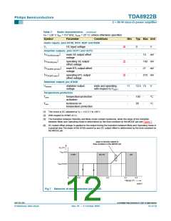
13. Application information
13.1 BTL application
When using the power amplifier in a mono BTL application the inputs of both channels
must be connected in parallel and the phase of one of the inputs must be inverted (see
Figure 6). In principle the loudspeaker can be connected between the outputs of the two
single-ended demodulation filters.
13.2 MODE pin
For pop-noise free start-up an RC time-constant must be applied on the MODE pin. The
bias-current setting of the VI-converter input is directly related to the voltage on the MODE
pin. In turn the bias-current setting of the VI converters is directly related to the DC output
offset voltage. Thus a slow dV/dt on the MODE pin results in a slow dV/dt for the DC
output offset voltage, resulting in pop-noise free start-up. A time-constant of 500 ms is
sufficient to guarantee pop-noise free start-up (see also Figure 4, 5 and 7).
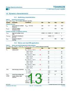
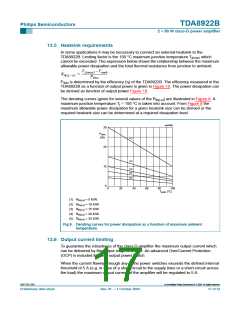
13.3 Output power estimation
The achievable output powers in several applications (SE and BTL) can be estimated
using the following expressions:
SE:
2
R
L
× V × (1 – t
× f
)
osc
-------------------
P
min
R + 0.6
L
P
=
(1)
-----------------------------------------------------------------------------------------
o(1%)
2 × R
L
9397 750 13357
© Koninklijke Philips Electronics N.V. 2004. All rights reserved.
Preliminary data sheet
Rev. 01 — 1 October 2004
15 of 32

 NXP [ NXP ]