TDA8922B
Philips Semiconductors
2 × 50 W class-D power amplifier
Table 9:
Stereo and dual SE application characteristics …continued
VP = ±26 V; RL = 6 Ω; fi = 1 kHz; RsL < 0.1 Ω [1]; Tamb = 25 °C; unless otherwise specified.
Symbol
Zi
Parameter
Conditions
Min
Typ
Max
Unit
input impedance
noise output voltage
45
68
-
kΩ
Vn(o)
operating
Rs = 0 Ω
mute
[5]
[6]
[7]
-
-
-
-
-
-
210
160
70
-
µV
µV
dB
dB
µV
dB
-
αcs
channel separation
channel unbalance
output signal in mute
-
∆Gv
-
1
-
[8]
Vo(mute)
CMRR
100
75
common mode rejection
ratio
Vi(CM) = 1 V (RMS)
-
[1] RsL is the series resistance of inductor of low-pass LC filter in the application.
[2] Output power is measured indirectly; based on RDSon measurement. See also Section 13.3.
[3] Total harmonic distortion is measured in a bandwidth of 22 Hz to 20 kHz, using an AES17 20 kHz brickwall filter. Maximum limit is
guaranteed but may not be 100 % tested.
[4] Vripple = Vripple(max) = 2 V (p-p); Rs = 0 Ω.
[5] B = 22 Hz to 20 kHz, using an AES17 20 kHz brickwall filter.
[6] B = 22 Hz to 20 kHz, using an AES17 20 kHz brickwall filter; independent of Rs.
[7] Po = 1 W; Rs = 0 Ω; fi = 1 kHz.
[8] Vi = Vi(max) = 1 V (RMS); fi = 1 kHz.
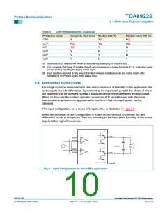
12.3 Mono BTL application
Table 10: Mono BTL application characteristics
VP = ±26 V; RL = 8 Ω; fi = 1 kHz; fosc = 317 kHz; RsL < 0.1 Ω [1]; Tamb = 25 °C; unless otherwise specified.
Symbol
Parameter
Conditions
Min
Typ
Max
Unit
[2]
[2]
[3]
Po
output power
RL = 6 Ω; VP = ±16 V
THD = 0.5 %
THD = 10 %
RL = 8 Ω; VP = ±21 V
THD = 0.5 %
THD = 10 %
Po = 1 W
-
-
48
60
-
-
W
W
-
-
71
88
-
-
W
W
THD
total harmonic distortion
closed loop voltage gain
fi = 1 kHz
-
0.02
0.07
36
0.05
-
%
fi = 6 kHz
-
%
Gv(cl)
35
37
dB
[4]
SVRR
supply voltage ripple
rejection
operating
fi = 100 Hz
-
80
80
80
80
34
-
-
-
-
-
dB
dB
dB
dB
kΩ
fi = 1 kHz
70
-
[4]
[4]
mute; fi = 100 Hz
standby; fi = 100 Hz
-
Zi
input impedance
22
9397 750 13357
© Koninklijke Philips Electronics N.V. 2004. All rights reserved.
Preliminary data sheet
Rev. 01 — 1 October 2004
14 of 32

 NXP [ NXP ]