Philips Semiconductors
Preliminary specification
Multi-purpose power amplifier
TDA8580J
V
handbook, full pagewidth
P
V
V
P2
P1
100 nF
1000 µF
3
15
IN1
IN2
IN3
IN4
IN5
OUT1+
OUT2−
OUT3−
OUT4+
1
4
7
8
inputs
(1)
14
17
10
11
12
V
switching
TDA8580J
(2)
(9 V typical)
2 Ω
BUFFER
9
(2)
220 nF
100 µF
STANDBY
R1
(3)
45 kΩ
10 kΩ
DIAG
+5 V
6
5
2
16
PGND1 PGND2
R2
(3)
MGS699
15 kΩ
4.7 µF
SW1
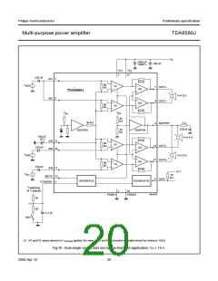
(1) Load conditions: quad SE (4 x 4 Ω), or dual BTL (2 x 8 Ω), or dual SE (2 x 4 Ω) and one BTL (1 x 8 Ω).
(2) RC combination not required in BTL mode.
(3) R1 and R2 values depend on Vswitching applied; the value of R1 and R2 connected in parallel should be minimum 10 kΩ.
Fig.31 Application 1; supply voltage range 8 V < VP ≤ 18 V; 1-pin and 2-pin operation.
V
handbook, full pagewidth
P
V
V
P2
P1
100 nF
1000 µF
3
15
IN1
IN2
OUT1+
OUT2−
OUT3−
OUT4+
1
4
7
8
inputs
IN3
(1)
14
17
10
11
12
13
5
IN4
V
switching
TDA8580J
(2)
(9 V typical)
2 Ω
IN5
BUFFER
9
(2)
220 nF
100 µF
4.7 µF
MUTE
STANDBY
R1
(3)
45 kΩ
DIAG
6
2
16
PGND1 PGND2
R2
(3)
15 kΩ
3.6 V
SW1
MGS697
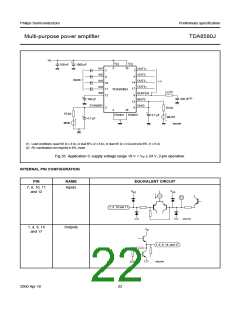
(1) Load conditions: quad SE (4 x 4 Ω), or dual BTL (2 x 8 Ω), or dual SE (2 x 4 Ω) and one BTL (1 x 8 Ω).
(2) RC combination not required in BTL mode.
(3) R1 and R2 values depend on Vswitching applied; the value of R1 and R2 connected in parallel should be minimum 10 kΩ.
Fig.32 Application 2; supply voltage range 18 V < VP ≤ 24 V; 1-pin operation.
2000 Apr 18
21

 NXP [ NXP ]