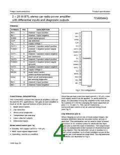
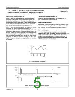
Philips Semiconductors
Product specification
2 × 25 W BTL stereo car radio power amplifier
with differential inputs and diagnostic outputs
TDA8566Q
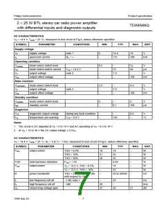
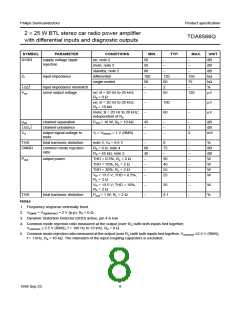
SYMBOL
PARAMETER
CONDITIONS
on; note 2
MIN.
TYP.
MAX.
UNIT
dB
SVRR
supply voltage ripple
rejection
50
50
80
−
−
−
−
mute; note 2
standby; note 2
differential
−
dB
dB
kΩ
kΩ
%
−
Zi
input impedance
100
50
−
120
60
2
150
75
single-ended
∆Zi
input impedance mismatch
noise output voltage
−
Vno
on; B = 20 Hz to 20 kHz;
−
85
120
µV
Rs = 0 Ω
on; B = 20 Hz to 20 kHz;
Rs = 10 kΩ
−
−
100
60
−
−
µV
µV
mute; B = 20 Hz to 20 kHz;
independent of Rs
αcs
∆Gv
Vo
channel separation
channel unbalance
Pout = 16 W; Rs = 10 kΩ
45
−
−
−
−
−
1
2
dB
dB
mV
output signal voltage in
mute
Vi = Vi(max) = 1 V (RMS)
−
THD
total harmonic distortion
note 3; V4 = 0.6 V
−
8
−
−
−
−
−
−
−
%
CMRR
common mode rejection
ratio
Rs = 0 Ω; note 4
60
40
−
75
−
dB
dB
W
W
W
W
Rs = 45 kΩ, note 5
THD = 0.5%; RL = 2 Ω
THD = 10%; RL = 2 Ω
THD = 30%; RL = 2 Ω
Pout
output power
30
40
55
25
−
−
VP = 13.5 V; THD = 0.5%;
−
RL = 2 Ω
VP = 13.5 V; THD = 10%;
RL = 2 Ω
−
−
35
−
−
W
%
THD
total harmonic distortion
P
out = 1 W; RL = 2 Ω
0.1
Notes
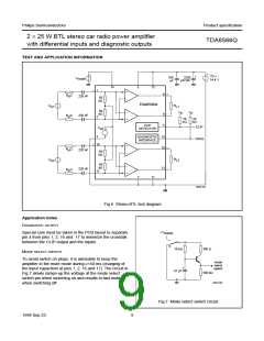
1. Frequency response externally fixed.
2. Vripple = Vripple(max) = 2 V (p-p), Rs = 0 Ω.
3. Dynamic Distortion Detector (DDD) active, pin 4 is low.
4. Common mode rejection ratio measured at the output (over RL) with both inputs tied together,
common ≤ 3.5 V (RMS), f = 100 Hz to 10 kHz, Rs = 0 Ω.
V
5. Common mode rejection ratio measured at the output (over RL) with both inputs tied together, Vcommon ≤3.5 V (RMS),
f = 1 kHz, Rs = 45 kΩ. The mismatch of the input coupling capacitors is excluded.
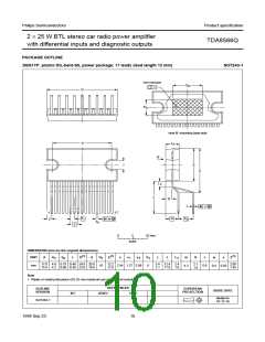
1998 Sep 23
8

 NXP [ NXP ]