Philips Semiconductors
Product specification
Full bridge vertical deflection output circuit
in LVDMOS with east-west amplifier
TDA8358J
Power dissipation calculation for the east-west stage
The required heatsink thermal resistance is given by:
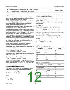
In general the shape of the east-west output wave form is
a parabola. The output voltage will be higher at the
beginning and end of the vertical scan compared to the
voltage at the scan middle, while the output current will be
higher at the scan middle. This results in an almost uniform
power dissipation distribution during scan. Therefore the
power dissipation can be calculated by multiplying the
average values of the output voltage and the output
current of pin OUTEW.
Tj – Tamb
Rth(h – a)
=
– ( R th(j – c) + Rth(c – h) )
------------------------
P
EW + PV
When we use the values known we find:
130 – 40
Rth(h – a)
=
– ( 4 + 1 ) = 5 K/W
----------------------
3 + 6
The heatsink temperature will be:
Th = Tamb + Rth(h-a) × Ptot = 40 + 5 × 9 = 85 °C
When verifying the dissipation also the start-up and stop
dissipation should be taken into account. Power
dissipation during start-up can be 3 to 5 times higher than
during normal operation.
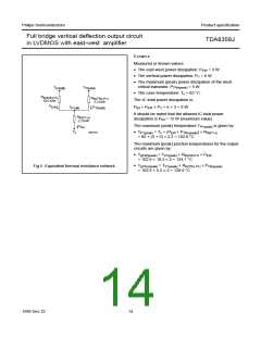
Equivalent thermal resistance network
The TDA8358J has two independent power dissipating
systems, the vertical output circuit and the east-west
circuit.
Heatsink calculation
It is recommended to verify the individual maximum (peak)
junction temperatures of both circuits. Therefore the
maximum (peak) power dissipations of the circuits and
also the heatsink temperature should be measured.
The maximum (peak) junction temperatures can be
calculated by using an equivalent thermal network
(see Fig.5).
The value of the heatsink can be calculated in a standard
way with a method based on average temperatures.
The required thermal resistance of the heatsink is
determined by the maximum die temperature of 150 °C.
In general we recommend to design for an average die
temperature not exceeding 130 °C. It should be noted
that the heatsink thermal resistance Rth(h-a) found by
performing a standard calculation will be lower then
normally found for a vertical deflection stand alone device,
due to the contribution of the EW power dissipation to this
value.
The network does only consist the contribution of the
maximum (peak) power dissipation PTRv(peak), being the
dissipation of the most critical transistor internally
connected to pins OUTB and VGND. The model assumes
equivalent maximum (peak) power dissipations during the
different vertical scan stages for all the functionally paired
transistors. The calculated maximum (peak) junction
temperatures should not exceed Tj = 150 °C.
EXAMPLE
Measured or known values:
PEW = 3 W; PV = 6 W; Tamb = 40 °C; Tj = 130 °C;
Rth(j-c) = 4 K/W; Rth(c-h) = 1 K/W.
1999 Dec 22
13

 NXP [ NXP ]