Philips Semiconductors
Preliminary specification
Video output amplifier
TDA6111Q
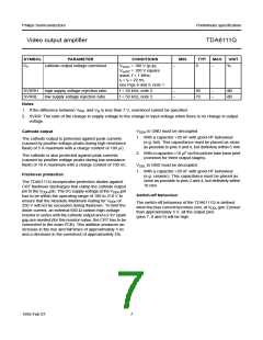
SYMBOL
PARAMETER
CONDITIONS
MIN.
TYP. MAX. UNIT
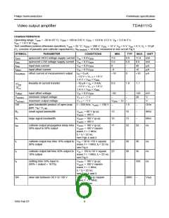
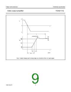
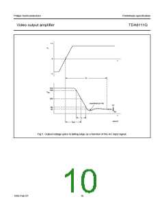
Ov
cathode output voltage overshoot
VocAC = 100 V (p-p);
VocDC = 100 V square
wave; f < 1 MHz;
−
9
−
%
tr = tf = 22 ns;
see Figs 4 and 5; note 1
SVRRH
SVRRL
high supply voltage rejection ratio
low supply voltage rejection ratio
f < 50 kHz; note 2
f < 50 kHz; note 2
−
−
85
70
−
−
dB
dB
Notes
1. If the difference between VDDL and Vip is less than 7 V, overshoot cannot be specified.
2. SVRR: The ratio of the change in supply voltage to the change in input voltage when there is no change in output
voltage.
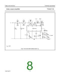
VDDH to GND must be decoupled:
Cathode output
1. With a capacitor >20 nF with good HF behaviour
(e.g. foil). This capacitance must be placed as close
as possible to pins 6 and 4, but definitely within 5 mm.
The cathode output is protected against peak currents
(caused by positive voltage peaks during high-resistance
flash) of 5 A maximum with a charge content of 100 µC.
2. With a capacitor >10 µF on the picture tube base print
The cathode is also protected against peak currents
(caused by positive voltage peaks during low-resistance
flash) of 10 A maximum with a charge content of 100 nC.
(common for three output stages).
VDDL to GND must be decoupled:
1. With a capacitor >20 nF with good HF behaviour
(e.g. ceramic). This capacitance must be placed as
close as possible to pins 2 and 4, but definitely within
10 mm.
Flashover protection
The TDA6111Q incorporates protection diodes against
CRT flashover discharges that clamp the cathode output
pin to the VDDH pin. The DC supply voltage at the VDDH pin
has to be within the operating range of 180 to 210 V to
ensure that the Absolute Maximum Rating for VDDH of
250 V will not be exceeded during flashover. To limit the
diode current, an external 680 Ω carbon high-voltage
resistor in series with the cathode output and a 2 kV spark
gap are needed (for this resistor-value, the CRT has to be
connected to the main PCB). This addition produces an
increase in the rise and fall times of approximately 5 ns
and a decrease in the overshoot of approximately 4%.
Switch-off behaviour
The switch-off behaviour of the TDA6111Q is defined:
when the bias current becomes zero, at VDDL (pin 2) lower
than approximately 5 V, all the output pins
(pins 7, 8 and 9) will be high.
1995 Feb 07
7

 NXP [ NXP ]