Philips Semiconductors
Preliminary specification
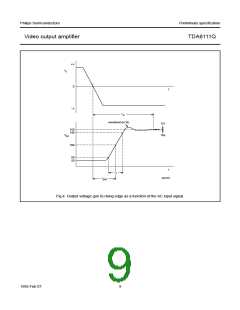
Video output amplifier
TDA6111Q
LIMITING VALUES
In accordance with the Absolute Maximum Rating System (IEC 134). Voltages measured with respect to GND (pin 4);
currents as specified in Fig.1; unless otherwise specified.
SYMBOL
VDDH
PARAMETER
CONDITIONS
MIN.
MAX.
250
UNIT
high level supply voltage
low level supply voltage
input voltage
0
0
0
V
V
V
V
VDDL
VI
14
VDDL
+6
VIdm
Vom
Voc
differential mode input voltage
measurement output voltage
cathode output voltage
feedback output voltage
input current
−6
0
VDDL
VDDH
VDDH
1
VDDL
VDDL
0
V
V
Vfb
Iin,Iip
IocsmL
mA
A
low non-repetitive peak cathode
output current
flashover discharge = 100 µC
0
5
IocsmH
high non-repetitive peak cathode
output current
flashover discharge = 100 nC
0
10
A
Ptot
Tstg
Tj
total power dissipation
storage temperature
junction temperature
electrostatic handling
human body model (HBM)
machine model (MM)
0
4
W
−55
−20
+150
+150
°C
°C
Ves
−
−
> 1500
> 400
V
V
HANDLING
Inputs and outputs are protected against electrostatic discharge in normal handling. However, to be totally safe, it is
desirable to take normal precautions appropriate to handling MOS devices (see “Handling MOS Devices”).
QUALITY SPECIFICATION
Quality specification “SNW-FQ-611 part E” is applicable, except for ESD Human body model see Chapter “Limiting
values”, and can be found in the “Quality reference handbook” (ordering number 9398 510 63011).
THERMAL CHARACTERISTICS
SYMBOL
Rth j-c
Note
1. External heatsink is required.
PARAMETER
VALUE
UNIT
thermal resistance from junction to case (note 1)
12
K/W
1995 Feb 07
5

 NXP [ NXP ]