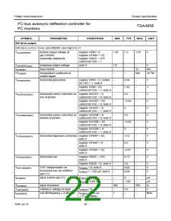
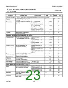
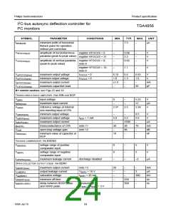
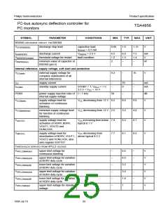
Philips Semiconductors
Product specification
I2C-bus autosync deflection controller for
PC monitors
TDA4856
Notes
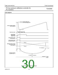
1. For duration of vertical blanking pulse see subheading ‘Vertical oscillator [oscillator frequency in application without
adjustment of free-running frequency ffr(V)]’.
2. Continuous blanking at CLBL (pin 16) will be activated, if one of the following conditions is true:
a) No horizontal flyback pulses at HFLB (pin 1) within a line
b) X-ray protection is triggered
c) Voltage at HPLL2 (pin 30) is low during soft start
d) Supply voltage at VCC (pin 10) is low
e) PLL1 unlocked while frequency-locked loop is in search mode.
3. Oscillator frequency is fmin when no sync input signal is present (continuous blanking at pins 16 and 17).
4. Loading of HPLL1 (pin 26) is not allowed.
5. Voltage at HPLL1 (pin 26) is fed to HBUF (pin 27) via a buffer. Disturbances caused by horizontal sync are removed
by an internal sample-and-hold circuit.
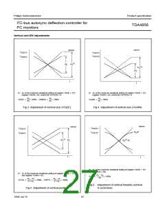
6. All vertical and EW adjustments according note 8, but VSIZE = 80% (register VSIZE = 63, VGAIN = 63 and control
bit VOVSCN = 0).
7. Value of resistor at VREF (pin 23) may not be changed.
8. All vertical and EW adjustments are specified at nominal vertical settings; unless otherwise specified, which means:
a) VSIZE = 100% (register VSIZE = 127, VGAIN = 63 and control bit VOVSCN = 0)
b) VSMOD = 0 (no EHT compensation)
c) VPOS centred (register VPOS = 64)
d) VLIN = 0 (register VLIN = X and control bit VSC = 1)
e) VLINBAL = 0 (register VLINBAL = 8)
f) FHMULT = 0
g) HPARAL = 0 (register HPARAL = 32)
h) HPINBAL = 0 (register HPINBAL = 32)
i) Vertical oscillator synchronized.
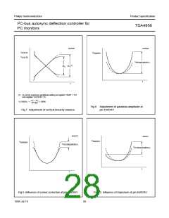
9. The output signal at EWDRV (pin 11) may consist of horizontal pincushion + corner correction + DC shift +
trapezium correction. If the control bit VOVSCN is set, and the VPOS adjustment is set to an extreme value, the tip
of the parabola may be clipped at the upper limit of the EWDRV output voltage range. The waveform of corner
correction will clip if the vertical sawtooth adjustment exceeds 110% of the nominal setting.
10. If fH tracking is enabled, the amplitude of the complete EWDRV output signal (horizontal pincushion + corner
correction + DC shift + trapezium) will be changed proportional to IHREF. The EWDRV low level of 1.2 V remains fixed.
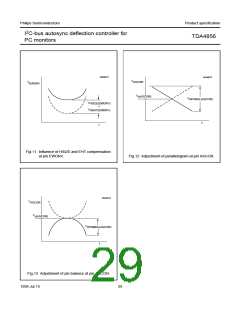
11. First pole of transconductance amplifier is 5 MHz without external capacitor (will become the second pole, if the OTA
operates as an integrator).
VBOP
12. Open-loop gain is
at f = 0 with no resistive load and CBOP = 10 nF [from BOP (pin 3) to GND].
-------------
VBIN
13. The recommended value for the pull-up resistor BDRV (pin 6) is 1 kΩ.
1999 Jul 13
26

 NXP [ NXP ]