Philips Semiconductors
Product specification
I2C-bus autosync deflection controller for
PC monitors
TDA4856
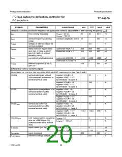
SYMBOL
tW(hfb)(off)
PARAMETER
CONDITIONS
MIN.
TYP.
7.5
MAX.
UNIT
µs
minimum width of horizontal
flyback pulse for operation
without pre-correction
−
−
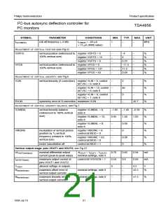
VHFOCUS(p-p)
amplitude of horizontal focus
parabola (peak-to-peak value)
register HFOCUS = 0
register HFOCUS = 31
−
−
−
0.06
3.3
−
−
−
V
V
V
VVFOCUS(p-p)
amplitude of vertical parabola register VFOCUS = 0;
0.02
(peak-to-peak value)
note 8
register VFOCUS = 15;
note 8
−
1.1
−
V
Vo(FOCUS)(max)
Vo(FOCUS)(min)
Io(FOCUS)(max)
CL(FOCUS)(max)
maximum output voltage
minimum output voltage
maximum output current
maximum capacitive load
IFOCUS = 0
IFOCUS = 0
6.15
1.0
±1.5
−
6.4
1.3
−
6.65
1.6
−
V
V
mA
pF
−
20
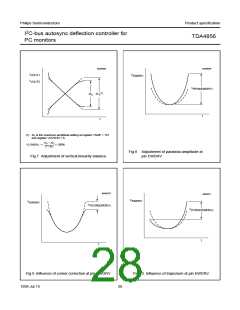
B+ control section; see Figs 22 and 23
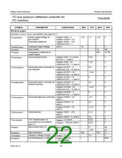
TRANSCONDUCTANCE AMPLIFIER: PINS BIN AND BOP
Vi(BIN)
input voltage
0
−
5.25
±1
V
Ii(BIN)(max)
Vref(int)
maximum input current
−
−
µA
V
reference voltage at internal
non-inverting input of OTA
2.37
2.5
2.58
Vo(BOP)(min)
Vo(BOP)(max)
Io(BOP)(max)
gm(OTA)
minimum output voltage
maximum output voltage
maximum output current
transconductance of OTA
open-loop voltage gain
−
−
0.5
5.6
−
V
IBOP < 1 mA
5.0
−
5.3
±500
50
86
−
V
µA
mS
dB
nF
note 11
note 12
30
−
70
−
Gv(ol)
CBOP(min)
minimum value of capacitor at
BOP
10
−
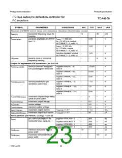
VOLTAGE COMPARATOR: PIN BSENS
Vi(BSENS)
voltage range of positive
comparator input
0
0
−
−
−
−
5
V
Vi(BOP)
voltage range of negative
comparator input
5
V
IL(BSENS)(max)
maximum leakage current
discharge disabled
−2
µA
OPEN-COLLECTOR OUTPUT STAGE: PIN BDRV
Io(BDRV)(max)
ILO(BDRV)
maximum output current
output leakage current
saturation voltage
note 13
20
−
−
−
mA
µA
mV
ns
VBDRV = 16 V
IBDRV < 20 mA
−
3
Vsat(BDRV)
−
−
300
−
toff(BDRV)(min)
td(BDRV-HDRV)
minimum off-time
−
250
500
delay between BDRV pulse
and HDRV pulse
measured at
VHDRV = VBDRV = 3 V
−
−
ns
1999 Jul 13
24

 NXP [ NXP ]