Philips Semiconductors
Product specification
I2C-bus autosync deflection controller for
PC monitors
TDA4856
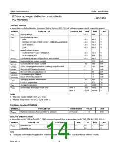
LIMITING VALUES
In accordance with the Absolute Maximum Rating System (IEC 134); all voltages measured with respect to ground.
SYMBOL
PARAMETER
CONDITIONS
MIN.
−0.5
MAX.
+16
UNIT
VCC
Vi(n)
supply voltage
input voltage on pins:
BIN
V
−0.5
−0.5
−0.5
−0.5
+6.0
+6.5
+8.0
+8.0
V
V
V
V
HSYNC, VSYNC, VREF, HREF, VSMOD and HSMOD
SDA and SCL
XRAY
Vo(n)
output voltage on pins:
VOUT2, VOUT1 and HUNLOCK
BDRV and HDRV
−0.5
−0.5
−0.5
−
+6.5
+16
+6.0
100
+10
−10
1
V
V
V
VI/O(n)
input/output voltages at pins BOP and BSENS
horizontal driver output current
horizontal flyback input current
video clamping pulse/vertical blanking output current
B+ control OTA output current
B+ control driver output current
Io(HDRV)
Ii(HFLB)
Io(CLBL)
Io(BOP)
Io(BDRV)
mA
mA
mA
mA
mA
mA
mA
°C
−10
−
−
−
50
Io(EWDRV) EW driver output current
Io(FOCUS) focus driver output current
−
−5
−
−5
Tamb
Tj
operating ambient temperature
junction temperature
−20
−
+70
150
+150
+150
+2000
°C
Tstg
VESD
storage temperature
−55
−150
−2000
°C
electrostatic discharge for all pins
note 1
note 2
V
V
Notes
1. Machine model: 200 pF; 0.75 µH; 10 Ω.
2. Human body model: 100 pF; 7.5 µH; 1500 Ω.
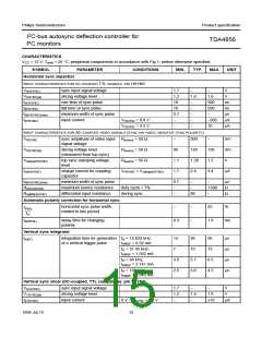
THERMAL CHARACTERISTICS
SYMBOL
PARAMETER
CONDITIONS
VALUE
55
UNIT
Rth(j-a)
thermal resistance from junction to ambient
in free air
K/W
QUALITY SPECIFICATION
In accordance with “URF-4-2-59/601”; EMC emission/immunity test in accordance with “DIS 1000 4.6” (IEC 801.6).
SYMBOL
PARAMETER
emission test
immunity test
CONDITIONS
MIN.
TYP.
1.5
2.0
MAX.
UNIT
mV
VEMC
note 1
note 1
−
−
−
−
V
Note
1. Tests are performed with application reference board. Tests with other boards will have different results.
1999 Jul 13
14

 NXP [ NXP ]