Philips Semiconductors
Product specification
4 x 11 W single-ended or 2 x 22 W power
amplifier
TDA1554Q
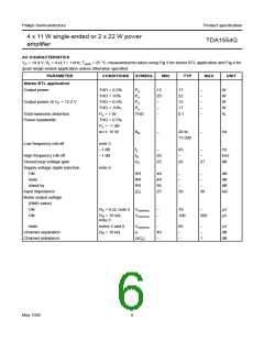
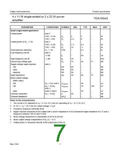
PARAMETER
CONDITIONS
SYMBOL
MIN.
TYP.
MAX.
UNIT
Quad single-ended application
Output power
note 7
THD = 0.5%
THD = 10%
note 7
P
P
4
5
6
−
−
W
W
o
o
5.5
Output power at R = 2 W
L
THD = 0.5%
THD = 10%
P
P
7.5
10
−
8.5
11
−
−
−
W
W
%
o
o
Total harmonic distortion
Low frequency roll-off
P = 1 W
THD
0.1
o
note 3
−3 dB
f
f
−
45
−
−
Hz
L
High frequency roll-off
−1 dB
20
19
−
kHz
dB
H
Closed loop voltage gain
G
20
21
v
Supply voltage ripple rejection
note 4
ON
RR
RR
RR
48
48
80
50
−
−
dB
dB
dB
kΩ
mute
−
−
stand-by
Input impedance
Noise output voltage
(RMS value)
ON
−
−
|Z |
60
75
i
R = 0 Ω; note 5
V
V
−
−
50
70
−
µV
µV
S
no(rms)
ON
R = 10 kΩ;
100
S
no(rms)
note 5
mute
notes 5 and 6
V
−
50
−
−
−
1
µV
dB
dB
no(rms)
Channel separation
Channel unbalance
R = 10 kΩ
α
40
−
S
|∆G |
−
v
Notes to the characteristics
1. The circuit is DC adjusted at V = 6 V to 18 V and AC operating at V = 8.5 V to 18 V.
P
P
2. At 18 V < V < 30 V the DC output voltage ≤ V /2.
P
P
3. Frequency response externally fixed.
4. Ripple rejection measured at the output with a source impedance of 0 Ω (maximum ripple amplitude of 2 V) and a
frequency between 100 Hz and 10 kHz.
5. Noise voltage measured in a bandwidth of 20 Hz to 20 kHz.
6. Noise output voltage independent of R (V = 0 V).
S
I
7. Output power is measured directly at the output pins of the IC.
May 1992
7

 NXP [ NXP ]