Philips Semiconductors
Product specification
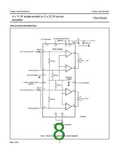
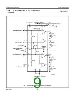
4 x 11 W single-ended or 2 x 22 W power
amplifier
TDA1554Q
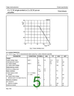
Fig.2 Power derating curve.
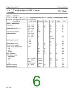
DC CHARACTERISTICS
V = 14.4 V; T = 25 °C; measurements taken using Fig.4; unless otherwise specified
P
amb
PARAMETER
CONDITIONS
SYMBOL
MIN.
TYP.
MAX.
UNIT
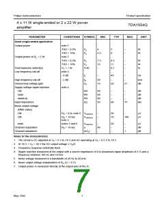
Supply
Supply voltage range
Total quiescent current
DC output voltage
note 1
V
6.0
14.4
18.0
V
P
I
−
−
−
80
6.9
−
160
−
mA
V
tot
note 2
V
O
DC output offset voltage
|∆V |
100
mV
O
Mute/stand-by switch
Switch-on voltage level
V
V
8.5
3.3
−
−
−
V
V
ON
6.4
Mute condition
mute
Output signal in mute
position
V = 1 V (max);
I
f = 1 kHz
V
−
−
2
mV
O
DC output offset voltage
(between pins 6 to 8 and 10 to 12)
|∆V |
−
−
−
100
2
mV
V
O
V
0
Stand-by condition
DC current in
sb
stand-by condition
Switch-on current
I
I
−
−
−
100
40
µA
µA
sb
12
sw
May 1992
5

 NXP [ NXP ]