Philips Semiconductors
Product specification
4 x 11 W single-ended or 2 x 22 W power
amplifier
TDA1554Q
PINNING
1
2
3
4
5
6
7
8
NINV1
INV1
GND
RR
non-inverting input 1
inverting input 1
9
n.c.
not connected
10 OUT3
11 GND2
12 OUT4
output 3
ground (signal)
power ground 2 (substrate)
output 4
supply voltage ripple rejection
positive supply voltage 1
output 1
V
13
V
positive supply voltage 2
mute/stand-by switch
not connected
P1
P2
OUT1
GND1
OUT2
14 M/SS
15 n.c.
power ground 1 (substrate)
output 2
16 INV2
17 NINV2
inverting input 2
non-inverting input 2
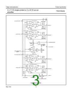
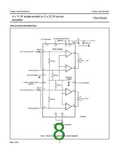
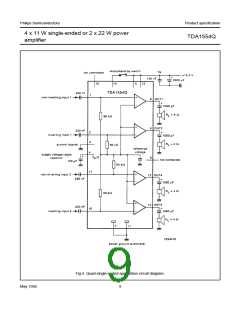
FUNCTIONAL DESCRIPTION
The TDA1554Q contains four identical amplifiers with differential input stages (two inverting and two non-inverting) and
can be used for single-ended or bridge applications. The gain of each amplifier is fixed at 20 dB (26 dB in BTL). A special
feature of this device is:
Mute/stand-by switch
• low stand-by current (< 100 µA)
• low mute/stand-by switching current (low cost supply switch)
• mute facility
RATINGS
Limiting values in accordance with the Absolute Maximum System (IEC 134)
PARAMETER
Supply voltage
CONDITIONS
SYMBOL
MIN.
MAX.
UNIT
operating
V
−
−
18
30
V
V
P
non-operating
load dump protected
V
P
during 50 ms;
t ≥ 2.5 ms
V
−
−
−
45
6
V
r
P
Non-repetitive peak output current
Repetitive peak output current
Storage temperature range
Junction temperature
I
I
A
OSM
4
A
ORM
T
T
−55
−
+ 150
150
18
°C
°C
V
stg
j
AC and DC short-circuit-safe voltage
Energy handling capability at outputs
Reverse polarity
V
−
PSC
V = 0 V
−
200
6
mJ
V
P
V
P
−
PR
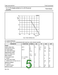
Total power dissipation
see Fig.2
−
60
W
tot
May 1992
4

 NXP [ NXP ]