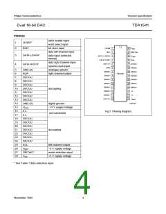
Philips Semiconductors
Product specification
Dual 16-bit DAC
TDA1541
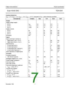
PARAMETER
Signal -to-noise ratio + THD*
Settling time to ± 1 LSB
Channel separation
SYMBOL
S/N
MIN.
TYP.
MAX.
UNIT
90
−
95
1
−
dB
µs
dB
dB
µs
tcs
α
−
80
−
tbf
0,1
−
−
Unbalance between outputs
Time delay between outputs
Power supply ripple rejection**
VDD = +5 V
∆IFS
td
0,2
1
−
RR
RR
RR
−
−
−
tbf
tbf
tbf
−
−
−
dB
dB
dB
VDD1 = −5 V
VDD2 = −15 V
Signal-to-noise ratio
at bipolar zero
S/N
−
−100
−
dB
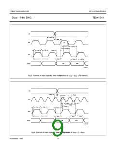
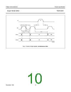
Timing (see Figs 3, 4 and 5)
Rise time
tr
−
−
−
−
−
−
−
−
−
−
−
−
−
−
−
−
−
−
−
35
35
−
ns
ns
ns
ns
ns
ns
ns
ns
ns
ns
ns
ns
ns
ns
ns
ns
ns
ns
Fall time
tf
−
Bit clock cycle time
tCY
160
48
48
0
Bit clock HIGH time
tHB
−
Bit clock LOW time
tLB
−
Bit clock fall time to latch rise time
Bit clock rise time to latch fall time
Data set-up time to bit clock
Data hold time to bit clock
Data set-up time to system clock
Word select hold time to system clock
Word select set-up time to system clock
tFBRL
tRBFL
tSDB
tHDB
tSDS
tHWS
tSWS
−
0
−
32
0
−
−
32
0
−
−
32
32
32
50
0
−
Bit clock fall time to system clock rise time tFBRS
System clock rise time to bit clock fall time tRSFB
System clock fall time to bit clock rise time tFSRB
Bit clock rise time to system clock fall time tRBFS
−
−
−
−
Latch enable LOW time
Latch enable HIGH time
tLLE
tHLE
20
32
−
−
* Signal-to-noise ratio + THD with 1 kHz full scale sinewave generated at a sampling rate of 176,4 kHz.
** Vripple = 1% of supply voltage and fripple = 100 Hz.
November 1985
8

 NXP [ NXP ]