Philips Semiconductors
Product specification
Signal-sources switch
TDA1029
Control inputs (pins 11, 12 and 13)
Required voltage
HIGH
(2)
V
>
<
3,3 V
SH
LOW
VSL
2,1 V
Input current
HIGH (leakage current)
LOW (control current)
I
<
<
1 µA
SH
−I
250 µA
SL
Notes
1. V
is typically 0,5 V
+ 1,5 V
.
10-16
14-16
BE
2. Or control inputs open (R
> 33 MΩ).
11,12,13−16
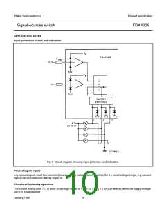
APPLICATION INFORMATION
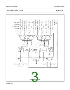
V = 20 V; T = 25 °C; measured in Fig.1; R = 47 kΩ; C = 0,1 µF; R
= 470 kΩ; R = 47 kΩ;
P
amb
S
i
bias
L
C = 100 pF (unless otherwise specified)
L
Voltage gain
G
typ.
typ.
−1,5 dB
10 mV
v
Output voltage variation when switching
the inputs
∆V
; ∆V
15−16
9−16
<
100 mV
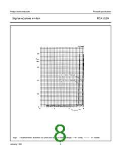
Total harmonic distortion
over most of signal range (see Fig.4)
d
d
d
typ.
typ.
typ.
0,01 %
0,02 %
0,03 %
tot
V = 5 V; f = 1 kHz
i
tot
tot
V = 5 V; f = 20 Hz to 20 kHz
i
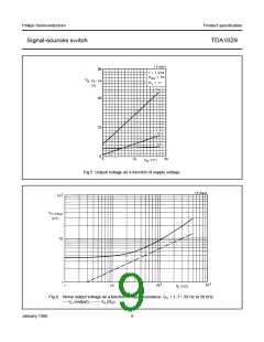
Output signal handling
>
5,0 V
5,3 V
d
= 0,1%; f = 1 kHz (r.m.s. value)
V
tot
o(rms)
typ.
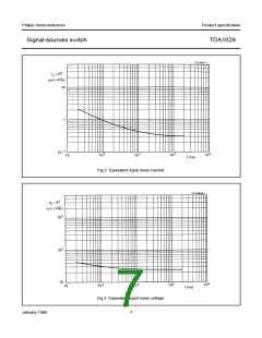
Noise output voltage (unweighted)
f = 20 Hz to 20 kHz (r.m.s. value)
Noise output voltage (weighted)
V
V
typ.
typ.
<
5 µV
n(rms)
f = 20 Hz to 20 kHz (in accordance with DIN 45405)
Amplitude response
12 µV
n
(1)
V = 5 V; f = 20 Hz to 20 kHz; C = 0,22 µF
∆V
∆V
0,1 dB
i
i
9-16;
15-16
Crosswalk between a switched-on input
and a non-switched-on input;
(2)
measured at the output at f = 1 kHz
Crosswalk between switched-on inputs
and the outputs of the other channels
α
α
typ.
typ.
75 dB
(2)
90 dB
Notes
1. The lower cut-off frequency depends on values of R
and C .
i
bias
2. Depends on external circuitry and R . The value will be fixed mostly by capacitive crosstalk of the external
S
components.
January 1980
6

 NXP [ NXP ]