Philips Semiconductors
Product specification
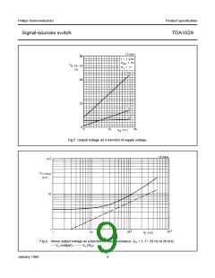
Signal-sources switch
TDA1029
RATINGS
Limiting values in accordance with the Absolute Maximum System (IEC 134)
Supply voltage (pin 14)
V
V
max.
max.
max.
23 V
P
Input voltage (pins 1 to 8)
V
P
I
−V
0,5 V
I
Switch control voltage (pins 11, 12 and 13)
Input current
V
0 to 23 V
S
±I
−I
max.
max.
max.
20 mA
I
Switch control current
50 mA
800 mW
S
Total power dissipation
P
tot
Storage temperature
T
T
−55 to + 150 °C
−30 to + 80 °C
stg
amb
Operating ambient temperature
CHARACTERISTICS
V = 20 V; T
= 25 °C; unless otherwise specified
P
amb
Current consumption
without load; I = I = 0
typ.
3,5 mA
2 to 5 mA
6 to 23 V
I
14
9
15
Supply voltage range (pin 14)
V
P
Signal inputs
Input offset voltage
of switched-on inputs
typ.
<
2 mV
10 mV
20 nA
V
io
R ≤ 1 kΩ
S
Input offset current
typ.
<
I
io
of switched-on inputs
200 nA
Input offset current
of a switched-on input with respect to a
non-switched-on input of a channel
Input bias current
typ.
<
20 nA
200 nA
I
I
io
typ.
<
250 nA
i
independent of switch position
Capacitance between adjacent inputs
D.C. input voltage range
950 nA
C
typ.
0,5 pF
V
3 to 19 V
100 µV/V
I
Supply voltage rejection ratio; R ≤ 10 kΩ
SVRR
typ.
typ.
typ.
S
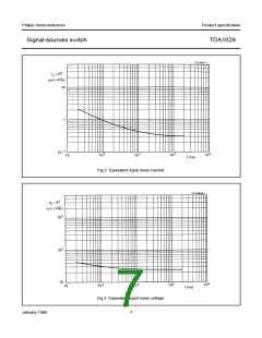
Equivalent input noise voltage
R = 0; f = 20 Hz to 20 kHz (r.m.s. value)
V
3,5 µV
S
n(rms)
Equivalent input noise current
f = 20 Hz to 20 kHz (r.m.s. value)
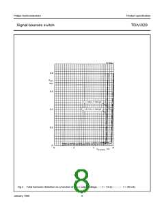
Crosstalk between a switched-on input
and a non-switched-on input;
I
0,05 nA
n(rms)
measured at the output at R = 1 kΩ; f = 1 kHz
α
typ.
100 dB
S
January 1980
4

 NXP [ NXP ]