Philips Semiconductors
Product specification
Signal-sources switch
TDA1029
Signal amplifier
Voltage gain of a switched-on input
at I = I = 0; R = ∞
G
G
typ.
typ.
1
9
15
L
v
5
Current gain of a switched-on amplifier
10
i
Signal outputs
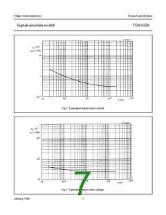
Output resistance (pins 9 and 15)
R
typ.
typ.
400 Ω
o
Output current capability at V = 6 to 23 V
±I ; ±I
5 mA
P
9
15
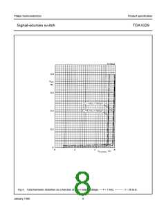
Frequency limit of the output voltage
V
= 1 V; R = 1 kΩ; R = 10 MΩ; C = 10 pF
f
typ.
typ.
1,3 MHz
i(p-p)
S
L
L
Slew rate (unity gain); ∆V
/∆t; ∆V
/∆t
9-16
15-16
R = 10 MΩ; C = 10 pF
S
2 V/µs
L
L
Bias voltage
(1)
D.C. output voltage
typ.
typ.
11 V
V
10-16
10,2 to 11,8 V
Output resistance
R
8,2 kΩ
10-16
Switch control
switched-on
inputs
interconnected
pins
control voltages
V
V
V
13-16
11-16
12-16
I-1, II-1
I-2, II-2
I-3, II-3
I-4, II-4
I-4, II-4
I-4, II-4
I-4, II-4
I-3, II-3
1-15, 5-9
2-15, 6-9
3-15, 7-9
4-15, 8-9
4-15, 8-9
4-15, 8-9
4-15, 8-9
3-15, 7-9
H
H
H
H
H
L
H
L
L
H
H
H
L
H
L
L
L
H
L
L
L
H
L
L
In the case of offset control, an internal blocking circuit of the switch control ensures that not more than one input will be
switched on at a time. In that case safe switching-through is obtained at V ≤ 1,5 V.
SL
January 1980
5

 NXP [ NXP ]