Philips Semiconductors
Product specification
Enhanced octal universal asynchronous
receiver/transmitter (Octal UART)
SCC2698B
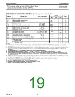
1, 2, 3, 4
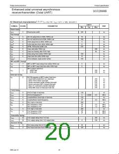
AC Electrical characteristics
T = 0 to +70_, V = 5.0 V " 10%, –40 to 85_C
A
CC
LIMITS
Typ
SYMBOL FIGURE
PARAMETER
UNIT
Max
Min
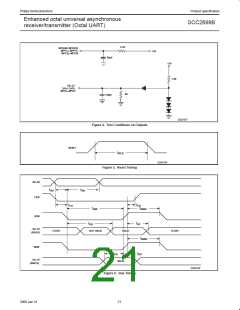
Reset timing
t
5
Reset pulse width
200
ns
RES
5
Bus timing
t
t
t
t
t
t
t
t
t
t
6
6
6
6
6
6
6
6
6
A0–A5 setup time to RDN, WRN Low
A0–A5 hold time from RDN, WRN Low
CEN setup time to RDN, WRN Low
CEN hold time from RDN, WRN High
WRN, RDN pulse width Low
10
100
0
ns
ns
ns
ns
ns
HS
AH
CS
CH
11
6
6
0
225
RW
DD
Data valid after RDN Low
200
80
ns
ns
ns
ns
ns
Data bus floating after RDN High
Data setup time before WRN High
Data hold time after WRN High
Time between reads and/or writes
DF
100
10
DS
DH
7
100
RWD
5
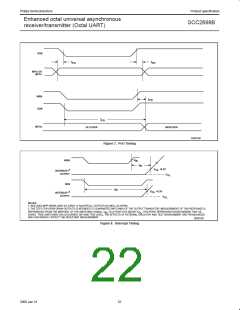
MPI and MPO timing
t
t
7
7
MPI or MPP input setup time before RDN Low
MPI or MPP input hold time after RDN High
0
0
ns
ns
PS
PH
MPO output valid from
WRN High
250
250
ns
ns
t
7
PD
RDN Low
Interrupt timing
t
IR
8
INTRN negated or MPP output High from:
Read RHR (RxRDY/FFULL interrupt)
Write THR (TxRDY interrupt)
Reset command (break change interrupt)
Reset command (MPI change interrupt)
Stop C/T command (counter interrupt)
Write IMR (clear of interrupt mask bit)
270
270
270
270
270
270
ns
ns
ns
ns
ns
ns
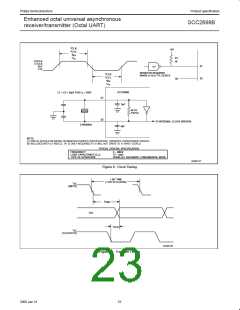
Clock timing
t
t
t
f
t
f
9
9
9
9
9
9
X1/CLK high or low time
120
0
ns
MHz
ns
CLK
CLK
CTC
CTC
RX
10
X1/CLK frequency
3.6864
4.0
4.0
Counter/timer clock high or low time
Counter/timer clock frequency
RxC high or low time
120
8
0
MHz
ns
200
8
RxC frequency (16X)
RxC frequency (1X)
0
2.0
1.0
MHz
MHz
RX
8
0
t
f
9
9
TxC high or low time
200
ns
TX
8
8
TxC frequency (16X)
TxC frequency (1X)
0
2.0
1.0
MHz
MHz
TX
0
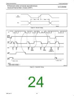
Transmitter timing
t
t
10
10
TxD output delay from TxC low
350
150
ns
ns
TXD
TCS
TxC output delay from TxD output data
0
Receiver timing
t
t
11
11
RxD data setup time to RxC high
RxD data hold time from RxC high
50
ns
ns
RXS
RXH
100
20
2000 Jan 31

 NXP [ NXP ]