Philips Semiconductors
Product specification
Enhanced octal universal asynchronous
receiver/transmitter (Octal UART)
SCC2698B
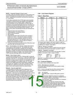
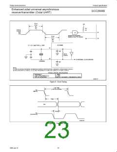
1, 2, 3
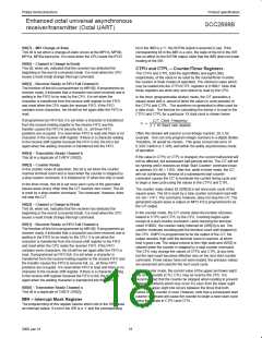
DC ELECTRICAL CHARACTERISTICS
T = 0 to +70_, V = 5.0 V " 10%, –40 to 85_C
A
CC
LIMITS
Typ
SYMBOL
PARAMETER
TEST CONDITIONS
UNIT
Max
Min
V
V
V
Input low voltage
Input high voltage (except X1/CLK)
Input high voltage (X1/CLK)
0.8
V
V
V
IL
2.0
IH
IH
0.8V
CC
I
= 2.4mA
= –400µA
= –100µA
0.4
V
V
V
OL
V
V
Output Low voltage
Output High voltage (except OD outputs)
OL
OH
I
I
0.8V
0.9V
OH
OH
CC
CC
I
I
Input current Low, MPI and MPP pins
Input current High, MPI and MPP pins
V
= 0
= V
CC
–50
µA
µA
IL
IH
IN
20
10
V
IN
I
I
Input leakage current
V
IN
= 0 to V
–10
µA
CC
I
I
X1/CLK input Low current
X1/CLK input High current
V
V
= GND, X2 = open
–100
µA
µA
ILX1
IHX1
IN
IN
= V , X2 = open
100
10
CC
I
I
Output off current High, 3-State data bus
Output off current Low, 3-State data bus
V
V
= V
IN
OZH
OZL
CC
–10
–10
µA
µA
= 0
IN
I
I
Open-drain output Low current in off state: IRQN
Open-drain output Low current in off state: IRQN
V
V
= V
ODL
ODH
IN
CC
= 0
10
30
IN
Power supply current
Operating mode
mA
mA
I
CC
9
Power down mode
2.0
NOTES:
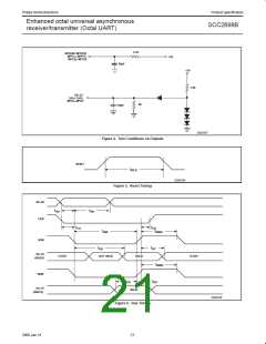
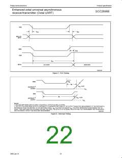
1. Parameters are valid over specified temperature range. See ordering information table for applicable temperature range and operating
supply range.
2. All voltage measurements are referenced to ground (GND). For testing, all inputs swing between 0.4V and 2.4V with a transition time of 20ns
maximum. For X1/CLK this swing is between 0.4V and 4.4V. All time measurements are referenced at input voltages of V and V , as
IL
IH
appropriate.
3. Typical values are at +25°C, typical supply voltages, and typical processing parameters.
4. Test condition for interrupt and MPP outputs: C = 50pF, R = 2.7kΩ to V . Test conditions for rest of outputs: C = 150pF.
L
L
CC
L
5. Timing is illustrated and referenced to the WRN and RDN inputs. The device may also be operated with CEN as the ‘strobing’ input. CEN
and RDN (also CEN and WRN) are ANDed internally. As a consequence, the signal asserted last initiates the cycle and the signal negated
first terminates the cycle.
6. If CEN is used as the ‘strobing’ input, the parameter defines the minimum high times between one CEN and the next. The RDN signal must
be negated for t
guarantee that any status register changes are valid.
RWD
7. Consecutive write operations to the command register require at least three edges of the X1 clock between writes.
8. This value is not tested, but is guaranteed by design.
9. See UART applications note for power down currents less than 5µA.
10.Operation to 0MHz is assured by design. Minimum test frequency is 2MHz.
11. Address is latched on leading edge of read or write cycle.
19
2000 Jan 31

 NXP [ NXP ]