Philips Semiconductors
Product specification
Dual asynchronous receiver/transmitter (DUART)
SCC2692
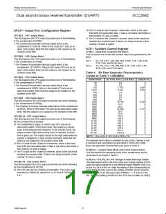
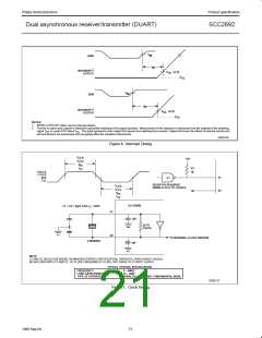
V
M
WRN
t
IR
1
INTERRUPT
V
+0.5V
OL
OUTPUT
V
OL
V
M
RDN
t
IR
1
INTERRUPT
V
+0.5V
OL
OUTPUT
V
OL
NOTES:
1. INTRN or OP3-OP7 when used as interrupt outputs.
2. The test for open-drain outputs is intended to guarantee switching of the output transistor. Measurement of this response is referenced from the midpoint of the switching
signal, V , to a point 0.5V above V . This point represents noise margin that assures true switching has occurred. Beyond this level, the effects of external circuitry and
M
OL
test environment are pronounced and can greatly affect the resultant measurement.
SD00136
Figure 6. Interrupt Timing
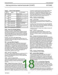
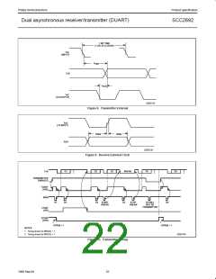
t
t
CLK
CTC
+5V
t
Rx
Tx
t
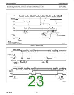
R1
1K
X1/CLK
CTCLK
RxC
X1
X2
U1
TxC
RESISTOR REQUIRED
WHEN U1 IS A TTL DEVICE
t
t
CLK
CTC
NC
t
Rx
t
Tx
SCC2698B
3pF
C1 = C2 = 24pF FOR C = 20PF
L
X1
X2
50 TO
150 KΩ
TO INTERNAL CLOCK DRIVERS
3.6864MHz
4pF
NOTE:
C1 AND C2 SHOULD BE BASED ON MANUFACTURER’S SPECIFICATION. PARASITIC CAPACITANCE SHOULD
BE INCLUDED WITH C1 AND C2. R1 IS ONLY REQUIRED IF U1 WILL NOT DRIVE TO X1 INPUT LEVELS
TYPICAL CRYSTAL SPECIFICATION
FREQUENCY:
LOAD CAPACITANCE (C ):
2 – 4MHZ
12 – 32pF
L
TYPE OF OPERATION:
PARALLEL RESONANT, FUNDAMENTAL MODE
SD00137
Figure 7. Clock Timing
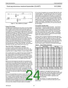
21
1998 Sep 04

 NXP [ NXP ]