PMBT3906
NXP Semiconductors
PNP switching transistor
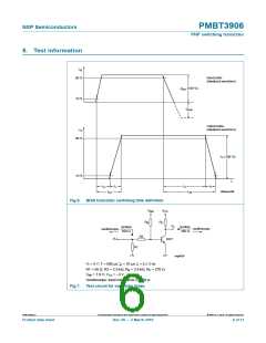
8. Test information
−
I
B
input pulse
90 %
(idealized waveform)
−
I
(100 %)
Bon
10 %
−
I
Boff
output pulse
−
(idealized waveform)
I
C
90 %
−
I
(100 %)
C
10 %
t
t
t
f
t
t
r
s
d
006aaa266
t
t
off
on
Fig 6. BISS transistor switching time definition
V
V
CC
BB
R
R
C
B
V
o
(probe)
(probe)
oscilloscope
oscilloscope
450 Ω
450 Ω
R2
V
I
DUT
R1
mgd624
VI = 5 V; T = 500 μs; tp = 10 μs; tr = tf ≤ 3 ns
R1 = 56 Ω; R2 = 2.5 kΩ; RB = 3.9 kΩ; RC = 270 Ω
VBB = 1.9 V; VCC = −3 V
Oscilloscope: input impedance Zi = 50 Ω
Fig 7. Test circuit for switching times
PMBT3906_6
All information provided in this document is subject to legal disclaimers.
© NXP B.V. 2010. All rights reserved.
Product data sheet
Rev. 06 — 2 March 2010
6 of 11

 NXP [ NXP ]