Philips Semiconductors
Preliminary data
Low power, low price, low pin count (20 pin)
microcontroller with 4 kbyte OTP
87LPC764
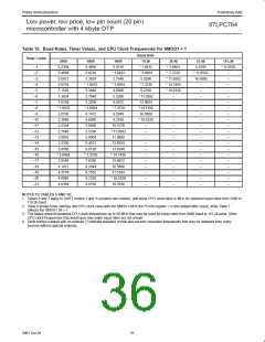
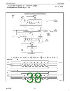
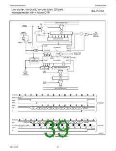
More About UART Modes 2 and 3
proves valid, it is shifted into the input shift register, and reception of
the rest of the frame will proceed.
Eleven bits are transmitted (through TxD), or received (through
RxD): a start bit (0), 8 data bits (LSB first), a programmable 9th data
bit, and a stop bit (1). On transmit, the 9th data bit (TB8) can be
assigned the value of 0 or 1. On receive, the 9the data bit goes into
RB8 in SCON. The baud rate is programmable to either 1/16 or 1/32
of the CPU clock frequency in Mode 2. Mode 3 may have a variable
baud rate generated from Timer 1.
As data bits come in from the right, 1s shift out to the left. When the
start bit arrives at the leftmost position in the shift register (which in
Modes 2 and 3 is a 9-bit register), it flags the RX Control block to do
one last shift, load SBUF and RB8, and set RI.
The signal to load SBUF and RB8, and to set RI, will be generated
if, and only if, the following conditions are met at the time the final
shift pulse is generated. 1. RI = 0, and 2. Either SM2 = 0, or the
received 9th data bit = 1.
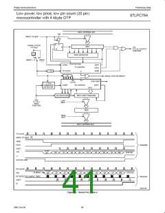
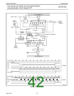
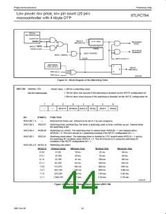
Figures 31 and 32 show a functional diagram of the serial port in
Modes 2 and 3. The receive portion is exactly the same as in Mode 1.
The transmit portion differs from Mode 1 only in the 9th bit of the
transmit shift register.
If either of these conditions is not met, the received frame is
irretrievably lost, and RI is not set. If both conditions are met, the
received 9th data bit goes into RB8, and the first 8 data bits go into
SBUF. One bit time later, whether the above conditions were met
or not, the unit goes back to looking for a 1-to-0 transition at the
RxD input.
Transmission is initiated by any instruction that uses SBUF as a
destination register. The “write to SBUF” signal also loads TB8 into
the 9th bit position of the transmit shift register and flags the TX
Control unit that a transmission is requested. Transmission
commences at S1P1 of the machine cycle following the next rollover
in the divide-by-16 counter. (Thus, the bit times are synchronized to
the divide-by-16 counter, not to the “write to SBUF” signal.)
Multiprocessor Communications
UART modes 2 and 3 have a special provision for multiprocessor
communications. In these modes, 9 data bits are received or
transmitted. When data is received, the 9th bit is stored in RB8. The
UART can be programmed such that when the stop bit is received,
the serial port interrupt will be activated only if RB8 = 1. This feature
is enabled by setting bit SM2 in SCON. One way to use this feature
in multiprocessor systems is as follows:
The transmission begins with activation of SEND, which puts the
start bit at TxD. One bit time later, DATA is activated, which enables
the output bit of the transmit shift register to TxD. The first shift pulse
occurs one bit time after that. The first shift clocks a 1 (the stop bit)
into the 9th bit position of the shift register. Thereafter, only zeros
are clocked in. Thus, as data bits shift out to the right, zeros are
clocked in from the left. When TB8 is at the output position of the
shift register, then the stop bit is just to the left of TB8, and all
positions to the left of that contain zeros. This condition flags the TX
Control unit to do one last shift and then deactivate SEND and set
TI. This occurs at the 11th divide-by-16 rollover after “write to SBUF.”
When the master processor wants to transmit a block of data to one
of several slaves, it first sends out an address byte which identifies
the target slave. An address byte differs from a data byte in that the
9th bit is 1 in an address byte and 0 in a data byte. With SM2 = 1, no
slave will be interrupted by a data byte. An address byte, however,
will interrupt all slaves, so that each slave can examine the received
byte and see if it is being addressed. The addressed slave will clear
its SM2 bit and prepare to receive the data bytes that follow. The
slaves that weren’t being addressed leave their SM2 bits set and go
on about their business, ignoring the subsequent data bytes.
Reception is initiated by a detected 1-to-0 transition at RxD. For this
purpose RxD is sampled at a rate of 16 times whatever baud rate
has been established. When a transition is detected, the
divide-by-16 counter is immediately reset, and 1FFH is written to the
input shift register.
SM2 has no effect in Mode 0, and in Mode 1 can be used to check
the validity of the stop bit, although this is better done with the
Framing Error flag. In a Mode 1 reception, if SM2 = 1, the receive
interrupt will not be activated unless a valid stop bit is received.
At the 7th, 8th, and 9th counter states of each bit time, the bit
detector samples the value of R–D. The value accepted is the value
that was seen in at least 2 of the 3 samples. If the value accepted
during the first bit time is not 0, the receive circuits are reset and the
unit goes back to looking for another 1-to-0 transition. If the start bit
37
2001 Oct 26

 NXP [ NXP ]