Philips Semiconductors
Preliminary specification
80C51 8-bit microcontroller
8K/256 OTP, 8 channel 10 bit A/D, I2C, PWM,
capture/compare, high I/O, low voltage (2.7V–5.5V), low power
P87C552
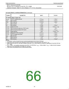
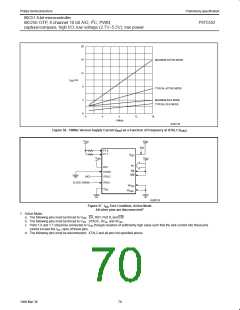
V
V
DD
DD
I
DD
P1.6
P1.7
V
DD
P0
RST
V
DD
STADC
EW
EA
(NC)
XTAL2
XTAL1
CLOCK SIGNAL
AV
SS
V
SS
AV
ref–
SU00219
Figure 58. I Test Condition, Idle Mode
DD
2
All other pins are disconnected
2. Idle Mode:
a. The following pins must be forced to V : Port 0 and EW.
DD
b. The following pins must be forced to V : RST, STADC, AV , AV , and EA.
SS
ss
ref–
c. Ports 1.6 and 1.7 should be connected to V through resistors of sufficiently high value such that the sink current into these pins
DD
cannot exceed the I
spec of these pins. These pins must not have logic 0 written to them prior to this measurement.
OL1
d. The following pins must be disconnected: XTAL2 and all pins not specified above.
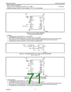
V
–0.5
DD
0.7V
DD
0.5V
0.2V
–0.1
DD
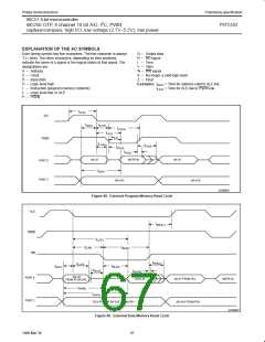
t
CHCX
t
t
CHCL
t
CLCX
CLCH
t
CLCL
SU00220
Figure 59. Clock Signal Waveform for I Tests in Active and Idle Modes
DD
t
= t
= 5ns
CHCL
CLCH
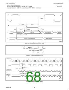
V
V
DD
DD
I
DD
P1.6
P1.7
V
DD
V
RST
DD
STADC
P0
EW
EA
(NC)
XTAL2
XTAL1
AV
SS
V
SS
AV
ref–
SU00221
Figure 60. I Test Condition, Power Down Mode
DD
3
All other pins are disconnected. V = 2V to 5.5V
DD
3. Power Down Mode:
a. The following pins must be forced to V : Port 0 and EW.
DD
b. The following pins must be forced to V : RST, STADC, XTAL1, AV , AV , and EA.
SS
ss
ref–
c. Ports 1.6 and 1.7 should be connected to V through resistors of sufficiently high value such that the sink current into these pins
DD
cannot exceed the I
spec of these pins. These pins must not have logic 0 written to them prior to this measurement.
OL1
d. The following pins must be disconnected: XTAL2 and all pins not specified above.
71
1999 Mar 30

 NXP [ NXP ]