NTAG213F/216F
NXP Semiconductors
NFC Forum T2T IC with 144/888 bytes user memory and field detection
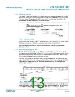
8.5.1 UID/serial number
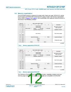
The unique 7-byte serial number (UID) and its two check bytes are programmed into the
first 9 bytes of memory covering page addresses 00h, 01h and the first byte of page 02h.
The second byte of page address 02h is reserved for internal data. These bytes are
programmed and write protected in the production test.
MSB
0
LSB
0
0
0
0
0
1
0
manufacturer ID for NXP Semiconductors (04h)
page 0
3
page 1
3
page 2
byte
0
1
2
0
1
2
0
1
2
3
serial number
part 1
serial number
part 2
check byte 1
check byte 0
internal
lock bytes
001aai001
Fig 8. UID/serial number
In accordance with ISO/IEC 14443-3 check byte 0 (BCC0) is defined as CT SN0 SN1
SN2 and check byte 1 (BCC1) is defined as SN3 SN4 SN5 SN6.
SN0 holds the Manufacturer ID for NXP Semiconductors (04h) in accordance with
ISO/IEC 14443-3.
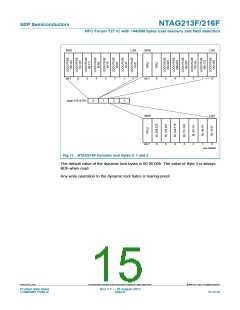
8.5.2 Static lock bytes (NTAG21xF)
The bits of byte 2 and byte 3 of page 02h represent the field programmable read-only
locking mechanism. Each page from 03h (CC) to 0Fh can be individually locked by setting
the corresponding locking bit Lx to logic 1 to prevent further write access. After locking,
the corresponding page becomes read-only memory.
The three least significant bits of lock byte 0 are the block-locking bits. Bit 2 deals with
pages 0Ah to 0Fh, bit 1 deals with pages 04h to 09h and bit 0 deals with page 03h (CC).
Once the block-locking bits are set, the locking configuration for the corresponding
memory area is frozen.
MSB
LSB
MSB
LSB
L
7
L
6
L
5
L
4
L
BL
BL
BL
CC
L
15
L
14
L
13
L
12
L
11
L
10
L
9
L
8
CC 15-10 9-4
page 2
0
1
2
3
lock byte 0
lock byte 1
Lx locks page x to read-only
BLx blocks further locking for the memory area x
aaa-006983
Fig 9. Static lock bytes 0 and 1
For example if BL15-10 is set to logic 1, then bits L15 to L10 (lock byte 1, bit[7:2]) can no
longer be changed. The so called static locking and block-locking bits are set by a WRITE
or COMPATIBILITY_WRITE command to page 02h. Bytes 2 and 3 of the WRITE or
NTAG213F_216F
All information provided in this document is subject to legal disclaimers.
© NXP B.V. 2013. All rights reserved.
Product data sheet
COMPANY PUBLIC
Rev. 3.1 — 28 August 2013
262231
13 of 56

 NXP [ NXP ]