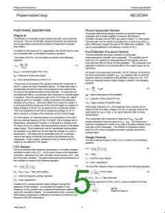
Philips Semiconductors
Product specification
Phase-locked loop
NE/SE564
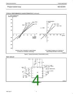
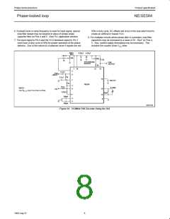
6. If pulsed burst or ramp frequency is used for input signal, special
loop filter design may be required in place of simple single
capacitor filter on Pins 4 and 5. (See PLL application section)
50% in duty cycle, DC offsets will occur in the loop which tend to
create an artificial or biased VCO.
8. For multiplier circuits where phase jitter is a problem, loop filter
capacitors may be increased to a value of 10 - 50µF on Pins 4,
5. Also, careful supply decoupling may be necessary. This
7. The input signal to Pin 6 and the VCO feedback signal to Pin 3
must have a duty cycle of 50% for proper operation of the phase
detector. Due to the nature of a balanced mixer if signals are not
includes the counter chain V lines.
CC
BIAS
ADJ
0.22µF 0.22µF
+5V
2k
10k
10k
1.2k
HYSTERESIS
ADJUST
FSK
OUTPUT
2k
1
10
15
16
2
6
0.1µF
0.1µF
FSK
INPUT
1k
14
7
10µF/8V
1k
NE564
3
9
510Ω
0–20pF
*NOTE:
12
+5V
Use R
only if rise time is critical.
9-11
*510Ω
33pF
11
13
8
300pF
4
5
300pF
SR01034
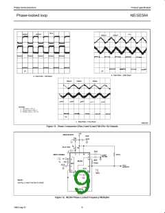
Figure 10. 10.8MHz FSK Decoder Using the 564
8
1994 Aug 31

 NXP [ NXP ]